Introduction to Chip Passivation Layers
In semiconductor chip manufacturing, the passivation layer is a critical thin film covering the chip surface, designed to protect internal structures from external environmental influences. It not only blocks moisture, dust, and chemical contaminants but also mitigates damage caused by mechanical stress and temperature fluctuations, significantly enhancing device reliability and lifespan. As chip technology continuously advances, the material and structural design of passivation layers have also become increasingly complex to meet the demands of higher performance and more stringent application scenarios.
Functions and Materials of Passivation Layers
The primary roles of a passivation layer include surface protection, mechanical shielding, interface passivation, and electrical insulation. Specifically, it effectively blocks external contaminants such as alkali metal ions and moisture, prevents electrochemical corrosion, reduces interface state density, improves channel mobility, and avoids short circuits between the gate and source. Furthermore, the passivation layer must possess good step coverage, material adhesion, and thermal stability to withstand various stress conditions encountered during manufacturing and in practical applications.
Common passivation layer materials are broadly categorized into inorganic and organic types. Inorganic materials, such as silicon dioxide (SiO₂) and silicon nitride (Si₃N₄), offer excellent insulating properties and density but have distinct advantages and disadvantages. Silicon dioxide has good compatibility with silicon substrates and low interface state density, but its structure is relatively porous with many pinholes, resulting in weaker barrier capability. Silicon nitride is hard, highly dense, and effective at blocking metal ion diffusion and moisture, but direct deposition on silicon can introduce a high density of surface states, adversely affecting device electrical performance.
Structure of Passivation Layers
As a single material often struggles to meet all performance requirements simultaneously, multi-layer passivation structures are commonly used in practice. For example, a combination of silicon dioxide and silicon nitride is frequently employed: silicon dioxide serves as an interfacial layer to reduce interface states, while silicon nitride acts as a barrier layer to prevent contaminant ingress. However, this dual-layer structure still has shortcomings, particularly the high brittleness of silicon nitride and its coefficient of thermal expansion mismatch with silicon, which can lead to micro-cracking under thermal stress.
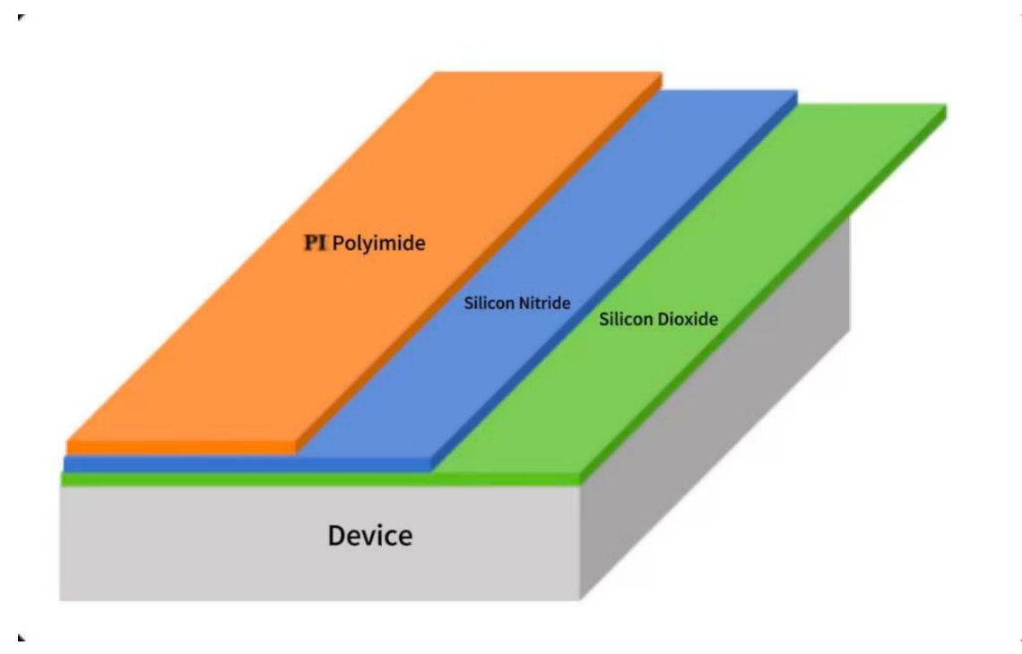
To further enhance reliability, the industry has introduced polyimide (PI) as an outer passivation material. Polyimide is a polymeric organic material characterized by high elastic modulus, low Young's modulus, high ductility, and low thermal stress. It effectively absorbs stress, preventing cracks in the underlying nitride layer. A three-layer passivation structure (SiO₂/Si₃N₄/PI) leverages the advantages of each material: the bottom SiO₂ layer provides interface passivation, the middle Si₃N₄ layer blocks ions and moisture, and the top PI layer offers mechanical buffering and resistance to physical damage.
Experiments show that this structure can reduce thermal stress by 50–70%, significantly decrease device resistance drift in humid environments, maintain low interface state density (<10¹¹ eV⁻¹cm⁻²), and deliver excellent performance in temperature cycling tests.
Other Passivation Materials
Besides SiO₂, Si₃N₄, and PI, various other materials are used for passivation layers with specific requirements.
Silicon-rich oxide (SRO) offers low interfacial stress and can serve as a stress buffer layer, but it has relatively low dielectric strength and may convert to SiO₂ at high temperatures. Silicon-rich nitride (SRN, SiOxNy) allows for stress tuning by adjusting the oxygen-to-nitrogen ratio, offering greater adaptability.
Phosphosilicate glass (PSG) and borophosphosilicate glass (BPSG) are doped glass materials known for their strong sodium ion gettering capability and good planarization effects. BPSG, doped with boron to lower its reflow temperature and phosphorus to improve moisture resistance, is commonly used in multi-layer structures.
Tetraethyl orthosilicate (TEOS), as a precursor for SiO₂ deposition, offers advantages such as excellent step coverage and low-temperature deposition but carries the risk of carbon residue.
These materials are typically selected or combined based on specific device structures, process compatibility, and application environments to achieve optimal passivation performance.
Importance of Passivation Layers
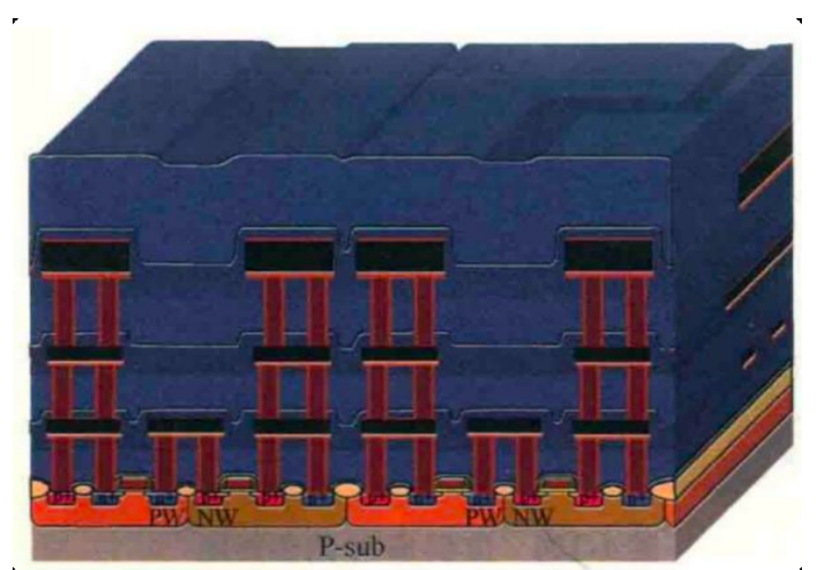
In devices such as power MOSFETs and IGBTs, the quality of the passivation layer directly impacts product performance in reliability tests (e.g., HTRB, HV-H3TRB). It covers the active area, metal layers, and termination regions, preventing external contamination and potential failure, making it a key factor in ensuring long-term stable operation.
In advanced packaging fields, such as Fan-Out Wafer-Level Packaging (FO-WLP), passivation layers must meet even stricter process requirements. Their curing temperature must be lower than the glass transition temperature of the molding compound (typically 150°C–175°C) to prevent material degradation. Furthermore, the passivation layer must exhibit good resolution, appropriate thickness, and smooth sidewall profiles to accommodate increasingly miniaturized and highly integrated chip structures and reduce stress concentration.
Specialists in high-precision measuring instruments often utilize tools like the white light interferometer to perform white light interferometry for non-contact, high-resolution measurement of passivation layer thickness, surface topography, and step coverage. This is crucial for quality control and ensuring the passivation layer meets strict design specifications in advanced packaging and power device manufacturing.
Although seemingly inconspicuous, the passivation layer is an indispensable component in modern chip manufacturing. The evolution from single inorganic layers to organic-inorganic composite multi-layer structures, along with advancements in materials and processes, continuously addresses challenges related to reliability, stress management, and contamination defense. Particularly in power devices and high-density packaging, optimized passivation layer design can significantly improve a device's environmental adaptability and lifespan. As semiconductor technology progresses towards smaller dimensions and higher performance, the importance of passivation layers will become even more pronounced, and innovations in their materials and structures will continue to drive improvements in chip reliability.

Boardstone lntelligent(Shenzhen)Co.,Ltd.
6F Building C Kaifa Plaza,7006 Caitian Rd.,Futian Dist,Shenzhen
Hotline:400 080 3885
Sales@atometrics.com.cn
WhatsApp: +86 13316897904


