I. Surface Roughness Measurement Methods and Main Equipment
Surface roughness measurement methods are diverse and can be primarily categorized into two types based on their principle: Contact and Non-contact. The specifics are as follows:
1. Contact Measurement Methods
Stylus Profilometry
Principle: A diamond stylus (with a tip radius of about 2 μm) traverses the surface. A displacement sensor records the profile undulations to calculate parameters like Ra and Rz.
Equipment: Electronic profilometer (portable or benchtop), CNC surface roughness measuring machine.
Characteristics: High accuracy (Ra 0.02–50 μm), but may scratch soft surfaces.
Replication Method (Molding)
Principle: Uses plastic materials (e.g., wax) to replicate the profile of hard-to-reach surfaces like deep holes or internal threads, followed by indirect measurement of the replica.
Equipment: Specialized replication material kit + profilometer.
2. Non-contact Measurement Methods
Optical Interferometry
Principle: Utilizes the deformation of optical interference fringes to deduce microscopic surface height variations, achieving nanometer-level resolution.
Equipment: White Light Interferometer (WLI), Interference Microscope.
Light Sectioning Method
Principle: A thin band of light is projected onto the surface, and the cross-sectional profile is observed through a microscope. Suitable for surfaces with Rz 0.8–100 μm.
Equipment: Light sectioning microscope (double-beam microscope).
Laser Scanning Method
Principle: A laser beam scans the surface, and changes in reflected light intensity or phase are analyzed.
Equipment: Laser profiler / scanner.
Atomic Force Microscopy (AFM)
Principle: A probe scans the surface, sensing inter-atomic forces to generate a 3D topography map.
Equipment: Atomic Force Microscope. Offers nanometer resolution but is slow and may potentially damage the sample.
3. Comparison Method
Principle: Roughness is assessed by visual or tactile comparison against standardized roughness reference samples. Fast but highly subjective, with low accuracy (only suitable for Ra > 2.5 μm).
The table below summarizes the key characteristics of the main measurement methods:
|
Measurement Method |
Measurement Range (Ra) |
Accuracy |
Characteristics |
Typical Equipment |
|
Stylus Profilometry |
0.02~50 μm |
High |
Contact, may scratch surface |
Mitutoyo CS-H5000 CNC |
|
White Light Interferometry |
Nanometer ~ Micrometer level |
Very High |
Non-contact, fast, 3D imaging |
Pomeas White Light Interferometer |
|
Light Sectioning |
0.8~100 μm |
Medium |
Manual point selection required, low efficiency |
Light Sectioning Microscope |
|
Atomic Force Microscopy (AFM) |
Nanometer level |
Very High |
Slow speed, may damage sample |
Atomic Force Microscope |
|
Comparison Method |
>2.5 μm |
Low |
Fast but subjective |
Roughness Comparison Specimens |
II. Overview of Main Measurement Equipment
1. Stylus-based Equipment
Mitutoyo Extreme SV-M3000 CNC: Supports large workpieces (e.g., engine blocks). X/Y-axis travel: 200/800 mm, drive speed: 200 mm/s, load capacity: 300 kg.
Mitutoyo CS-H5000 CNC: Integrates profile and roughness measurement. X-axis resolution: 5 nm. Suitable for high-precision workpieces like aspheric lenses.
2. Optical Non-contact Equipment
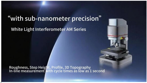
White Light Interferometer (WLI): Such as the Pomeas 3D Interferometer, supports analysis of 300+ parameters (e.g., Sa, Sq).
Trimos TR-Scan: Utilizes digital holographic microscopy technology, resistant to vibration interference. Can switch between confocal and stylus modules.
3. Microscopic Imaging Equipment
Atomic Force Microscope (AFM): Nanometer-level resolution, suitable for materials science research.
Interference Microscope: Traditional interferometry equipment, complex adjustment.
III. Core Advantages and Application Fields of White Light Interferometers
Due to their unique optical design and technology integration, White Light Interferometers have become the preferred tool for high-precision surface measurement.
Core Advantages
Ultra-High Precision and Repeatability: Vertical resolution reaches 0.1 nm, repeatability error < 1%. Superior to stylus methods (affected by measuring force) and traditional interferometry (requires manual fringe adjustment).
Non-contact, Non-destructive Measurement: No mechanical contact, avoids scratching ultra-smooth surfaces (e.g., wafers, optical lenses).
Efficient 3D Panoramic Imaging: Generates 3D topography in a single scan. Supports 300+ parameters per ISO 25178 (e.g., Sa, Sq, Smr), whereas stylus methods only acquire 2D profiles.
Resistance to Environmental Interference: Optical vibration isolation tables (e.g., TMC) and fast scanning technology (millisecond single-frame acquisition) suppress vibration effects.
Broad Applicability: Compatible with surfaces from ultra-smooth (Ra < 0.1 nm) to rough (Ra > 1 μm), and materials with high or low reflectivity.
Key Application Industries
Semiconductor Manufacturing:
Wafer roughness inspection (affects thin-film deposition quality), Thin-film thickness measurement (accuracy ±1 nm), Defect identification (cracks/bubbles).
Optical Component Processing:
Surface profile and coating quality analysis of lenses/prisms, ensuring optical path accuracy.
Precision Machinery and Automotive:
Tool wear monitoring, Batch inspection of surface roughness for crankshafts/cylinder blocks.
Materials Science Research:
Surface topography of nanomaterials, Coating uniformity, Microstructure volume calculation.
Biomedical:
3D topography analysis of cell morphology, biomolecular interactions.
Typical Equipment Parameter Example
Optical Configuration: Nikon interference objective, PI nano-positioning stage.
Software System: NanoWare (compliant with ISO/ASME standards, etc.), supports automatic report generation.
Measurement Speed: Single point measurement ≤ 1 second, full-field 3D scan < 5 minutes.
Summary
White Light Interferometers are irreplaceable in high-end manufacturing (especially semiconductors and optics) due to their nanometer-level precision, non-contact safe measurement, and comprehensive 3D analysis capabilities. For conventional industrial scenarios (e.g., workshop quality inspection), stylus profilometers (like the Mitutoyo series) remain an efficient choice. For deep holes or soft materials, the replication method is more practical. Technology selection requires comprehensive consideration of accuracy requirements, sample characteristics, and cost.

Boardstone lntelligent(Shenzhen)Co.,Ltd.
6F Building C Kaifa Plaza,7006 Caitian Rd.,Futian Dist,Shenzhen
Hotline:400 080 3885
Sales@atometrics.com.cn
WhatsApp: +86 13316897904


