Ⅰ Functions and Advantages of Atometrics Super Large Depth of Field Digital Microscope:
Main Functions:
1. Imaging & Focusing: Intelligent imaging with an super large depth of field; full-frame auto-focusing achievable in as fast as 1 second.
2. Measurement & Analysis: One-click observation and analysis; built-in 30+ measurement tools for performing measurements and annotations.
3. Save & Share: One-click saving and sharing of images and measurement data.
4. Customization: Supports various customized functions to meet the needs of different scenarios.
Equipment Advantages:
1. High Pixel Count: 12 Megapixel ultra-high effective pixel count, research-grade high resolution.
2. Superior Optical Design: Newly designed optical path with 50+ lens groups.
3. Rich Functionality: Supports functions such as metallographic analysis, non-metallic inclusion assessment, and cleanliness analysis.
4. Diverse Platforms: Can be equipped with different stages to meet various sample observation needs.
Ⅱ The depth of field of an super large depth of field digital microscope is significantly improved compared to a conventional optical microscope, as detailed below:
1. Magnitude of Improvement: The depth of field of a conventional optical microscope is typically between 2-3μm. In contrast, the depth of field of an super-depth-of-field microscope can reach several tens of millimeters. For example, some super-depth-of-field microscopes can achieve a depth of field of 20mm at 500x magnification, which is 40 times greater than the depth of field of a conventional microscope (0.5mm) at the same magnification. Models like the VHX-5000 super-depth-of-field microscope can achieve a maximum depth of field of 34mm, representing an extremely significant improvement.
2. Principle of Improvement: Conventional optical microscopes have a shallow depth of field, only clearly imaging a single focal plane, requiring frequent refocusing for uneven samples. Super-depth-of-field microscopes extend the depth of field through various technologies. In terms of optical design, they use high numerical aperture objectives and aperture diaphragms, adjusting the light source spot size and diaphragm position to vary the focus of light rays at different depths. Simultaneously, combined with software algorithms—such as multi-focal plane image stacking or focus variation methods—images from different focal planes are fused into a fully focused image. Furthermore, through Z-axis scanning, either the stage or the objective is moved to scan the sample layer-by-layer along the Z-axis, acquiring a sequence of 2D images from different focal planes. Subsequent 3D reconstruction then significantly increases the depth range that can be imaged clearly.
Ⅲ Application Industries for Super Large Depth of Field Digital Microscopes
Leveraging its unique large depth of field, high resolution, and 3D imaging capabilities, the ultra-depth-of-field microscope finds widespread application across multiple industries. Below are some of the main application sectors:
1. Biomedical Field: Used for observing and analyzing the microstructure and characteristics of biological samples such as cells, tissues, and microorganisms. Through high-resolution 3D images, researchers can gain deeper insights into the morphology, structure, and function of biological samples, providing crucial evidence for disease diagnosis, treatment, and drug development. Examples include observing the morphology and distribution of organelles within cells, analyzing lesion areas in tissue sections, and studying the growth and reproduction processes of microorganisms.
2. Materials Science Field: Used for observing and analyzing the surface morphology, microstructure, and defects of materials. Through high-precision measurement and analysis, researchers can evaluate material properties and quality, providing essential support for material R&D, production, and application. For instance, observing the grain size and grain boundary structure of metal materials, analyzing internal pores and cracks in ceramic materials, and studying the micro-phase structure of polymer materials.
3. Electromechanical Engineering Field: Used for observing and analyzing the surface morphology, dimensional accuracy, and defects of small objects such as mechanical parts and electronic components. Through high-precision measurement and analysis, researchers can assess product quality and performance, providing important references for product improvement and optimization. Examples include detecting wear and scratches on the surface of mechanical parts, observing the soldering quality of electronic component leads, and measuring the dimensional accuracy of tiny parts.
4. 3D Printing Field: Used for observing and analyzing the surface morphology, dimensional accuracy, and internal structure of 3D printed products. Through high-precision measurement and analysis, researchers can evaluate the feasibility and reliability of 3D printing technology, providing significant support for its development and application. For example, observing the stair-step effect and roughness on the surface of 3D printed products, analyzing the bonding between printed layers, and measuring the size and distribution of internal pores.
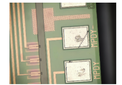
5. Integrated Circuit Field: Used for observing and analyzing the surface morphology, microstructure, and defects of chips. For example, inspecting whether the lithography patterns on the chip surface are clear, analyzing the internal circuit structure and connections of the chip, and identifying defects and impurities introduced during the chip manufacturing process.
6. Archaeology Field: Used for observing and analyzing the microstructure and characteristics of archaeological samples such as cultural relics and site materials. Through high-resolution 3D images, researchers can gain deeper understanding of the craftsmanship, material sources, and preservation status of artifacts, providing vital support for their conservation and study. Additionally, it can be used to observe and analyze tiny remains and artifacts at excavation sites, offering important clues for archaeological research. Examples include observing the body structure and glaze characteristics of ancient ceramics, and analyzing the corrosion status and manufacturing techniques of metal artifacts.
7. Botany Field: Used for observing and analyzing the microstructure and characteristics of biological samples such as plant cells, tissues, and organs. Through high-resolution 3D images, researchers can gain deeper insights into plant growth, development, and physiological/biochemical processes, providing important support for botanical research and applications. For example, observing the cell wall structure and organelle distribution in plant cells, and analyzing the vascular bundle system and stomatal structure in plant tissues.
The Atometrics AH Series Super Large Depth of Field Digital Microscope allows for 360-degree, high-definition observation and analysis of surface defects, micro-morphology, material metallographic structure, flaws/abnormalities, failure analysis, 2D/3D micro-measurements, etc. With a pixel count as high as 12 Megapixels, it enables one-click full-frame focusing, observation, and measurement.

Boardstone lntelligent(Shenzhen)Co.,Ltd.
6F Building C Kaifa Plaza,7006 Caitian Rd.,Futian Dist,Shenzhen
Hotline:400 080 3885
Sales@atometrics.com.cn
WhatsApp: +86 13316897904


