In the process of industrializing MicroLED, luminous efficiency and beam shaping control are two unavoidable technical hurdles. Microlens arrays (MLAs), as an optical solution that simultaneously improves light extraction efficiency and beam shaping, are receiving increasing attention from the industry. At the same time, as MLA technology gradually moves towards mass production, how to efficiently and accurately perform full-scale testing of micron-level lenses has become a new challenge for the industry chain.
I. Why Does MicroLED Need Microlens Technology?
MicroLED, with its high brightness, high contrast, and fast response speed, is considered an important direction for next-generation display technology. However, at the micron-level chip scale, a fundamental physical problem has always limited its performance ceiling—low light extraction efficiency.
Due to the large difference in refractive index between semiconductor materials such as GaN and air, a large number of photons are confined inside the chip under total internal reflection conditions and are ultimately absorbed and lost by the material. Industry data shows that the light extraction efficiency of MicroLEDs in bare chip form is often less than 30%, with most of the light energy wasted.
On the other hand, in emerging scenarios such as AR/VR near-eye displays, automotive HUDs, and micro-projections, MicroLEDs not only need to output sufficient brightness but also require precise control of the light emission angle. Traditional LEDs have a Lambertian distribution with a half-divergence angle of approximately ±60°. This diffuse characteristic can cause energy loss and pixel crosstalk in waveguide coupling and optical engine scenarios.
Microlens arrays provide a feasible optical solution for MicroLEDs in two dimensions: "improving luminous efficiency" and "beam shaping."
II. Core Value and Technical Challenges of Microlens Arrays
The value of microlens arrays is mainly reflected in two aspects: first, improving light extraction efficiency by changing the incident angle at the interface, allowing more photons to escape from the chip; different solutions can bring luminous efficiency improvements ranging from 20% to 80%; second, achieving beam shaping by compressing divergent light into a directional beam, increasing axial light intensity by more than two times. Some combined structures can control the full width at half maximum (FWHM) within ±10°, effectively reducing pixel crosstalk.
Currently, mainstream fabrication methods include grayscale photolithography, nanoimprint lithography, dry etching, thermal reflow, and inkjet printing, each with its own focus. However, industrialization still faces multiple challenges: micron-level alignment precision requirements, balancing the compatibility of high-refractive-index materials and processes, and controlling yield and cost in wafer-level mass production are all areas where the industry needs continuous breakthroughs.
III. Mass Production Inspection: A Key Link to the Deployment of Microlens Arrays
When microlens arrays move from the laboratory to the production line, quality inspection becomes the core link to ensure yield and consistency. This link is far more difficult than the inspection of conventional optical components because the scale and specifications of the objects being inspected vary greatly.
An 8-inch wafer typically contains tens of thousands of microlenses, each requiring independent inspection. Evaluation metrics encompass multiple dimensions: Radius of curvature (ROC) determines the lens's focusing ability and focal length, directly impacting the design and matching of the optical system; surface roughness (Ra/Sa) relates to light scattering loss and requires nanometer-level precision; aspherical K-value and surface profile deviation (SPD) reflect the degree of agreement between the lens morphology and design values; and lens pitch affects the array's fill factor and optical uniformity.
Among these metrics, the lens itself is micrometer-scale, while surface roughness requires nanometer-scale resolution. Traditional inspection methods often face a dilemma: high-precision equipment is slow, making it difficult to support the production capacity demands of full wafer inspection; solutions prioritizing efficiency may compromise on nanometer-level precision. For mass production lines, balancing accuracy and efficiency is a real challenge.
IV. Atometrics NX230 Series: Full Inspection Solution for Wafer MLAs
Addressing the full inspection needs of wafer-level microlens arrays, Ucotest has launched the NX230 series of wafer 3D automated measurement equipment, providing an integrated solution for MLA mass production inspection.
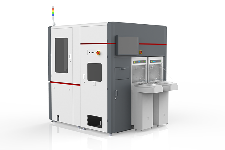
Multi-Technology Integrated Inspection Architecture
The NX230 series adopts a modular design, featuring a standard wafer adsorption stage and integrating two main measurement units: a white light interferometer and a spectral confocal displacement sensor. The white light interferometer module is equipped with a high-precision piezoelectric ceramic scanning structure, coupled with a high-sensitivity, high-pixel CMOS camera, enabling rapid acquisition of high-density 3D point cloud data. Combined with SST and GAT algorithms, the equipment can complete the acquisition and processing of large amounts of data points in a short time, providing a foundation for nanometer-level precision inspection of micron-level morphology.
Fully Automated Inspection Capability
The equipment supports a fully automated inspection process, encompassing functions such as automatic focusing, automatic positioning, and automatic positioning. After the operator loads the wafer, the equipment can sequentially traverse each lens according to a preset path, eliminating the need for manual intervention. After scanning each lens, the system automatically outputs inspection data and performs pass/fail judgment based on preset thresholds, distinguishing between good and defective products.
Furthermore, the equipment also supports a grading and sorting function, classifying lenses into different grades according to performance indicators based on measurement data, facilitating targeted selection in downstream processes. The generated 3D thermal map visually presents the parameter distribution trend of the entire wafer, helping process engineers quickly locate yield fluctuation areas and providing data support for process optimization.
Comprehensive Inspection Index Coverage
The NX230 series can inspect items covering the core evaluation dimensions of microlens arrays, including: radius of curvature (ROC), numerical aperture (NA), surface roughness (Ra/Sa, etc.), aspherical K-value, surface profile deviation (SPD), and lens pitch. The inspection time for a single lens is approximately 10 seconds, representing a significant improvement in overall efficiency compared to traditional manual inspection methods, effectively meeting the cycle time requirements of full inspection on mass production lines.
According to publicly available case studies, after introducing this equipment, the Fuzhou factory of an international materials brand saw improvements in the efficiency and stability of wafer MLA full inspection, providing reliable quality assurance for large-scale production.
Microlens arrays, as an important technological direction for the optical upgrade of MicroLEDs, are gradually moving from the laboratory to industrial applications. In this process, fabrication technology and testing technology complement each other—only by establishing an efficient and accurate mass production testing system can the large-scale deployment of microlens arrays be truly supported. With the continuous improvement of testing solutions, microlens arrays are expected to unleash greater application value in emerging fields such as MicroLED and AR displays. Multi-Technology Integrated Testing Architecture
The NX230 series adopts a modular design, featuring a standard wafer adsorption stage and integrating two major measurement units: a white light interferometer and a spectral confocal displacement sensor. The white light interferometer module is equipped with a high-precision piezoelectric ceramic scanning structure, coupled with a high-sensitivity, high-pixel CMOS camera, enabling rapid acquisition of high-density 3D point cloud data. Combined with SST and GAT algorithms, the equipment can complete the acquisition and processing of a large number of data points in a short time, providing a foundation for nanometer-level precision detection of micron-level morphology.
Fully Automated Testing Capability
The equipment supports a fully automated testing process, covering functions such as automatic focusing, automatic positioning, and automatic repositioning. After the operator loads the wafer, the equipment can sequentially traverse each lens according to a preset path, without requiring manual intervention for each lens individually. After scanning each lens, the system automatically outputs inspection data and determines whether it is good or defective based on preset thresholds.
Furthermore, the equipment supports a tiered sorting function, classifying lenses into different grades according to performance indicators based on measurement data, facilitating targeted selection by downstream processes. Simultaneously, the generated 3D thermal map visually presents the parameter distribution trend of the entire wafer, helping process engineers quickly locate yield fluctuation areas and providing data support for process optimization.
Comprehensive Inspection Index Coverage
The NX230 series can inspect items covering the core evaluation dimensions of microlens arrays, including: radius of curvature (ROC), numerical aperture (NA), surface roughness (Ra/Sa, etc.), aspherical K-value, surface profile deviation (SPD), and lens pitch. The inspection time for a single lens is approximately 10 seconds, representing a significant improvement in overall efficiency compared to traditional manual inspection methods, effectively meeting the cycle time requirements of full inspection on mass production lines.
Publicly available case studies show that after introducing this equipment, a certain international materials brand's Fuzhou factory experienced improvements in the efficiency and stability of its full-scale wafer MLA inspection, providing reliable quality assurance for large-scale production.
Microlens arrays, as a crucial technological direction for upgrading MicroLED optics, are gradually moving from the laboratory to industrial applications. In this process, fabrication processes and testing technologies complement each other—only by establishing an efficient and accurate mass production testing system can the large-scale deployment of microlens arrays be truly supported. With the continuous improvement of testing solutions, microlens arrays are expected to unleash greater application value in emerging fields such as MicroLED and AR displays.

Boardstone lntelligent(Shenzhen)Co.,Ltd.
6F Building C Kaifa Plaza,7006 Caitian Rd.,Futian Dist,Shenzhen
Hotline:400 080 3885
Sales@atometrics.com.cn
WhatsApp: +86 13316897904