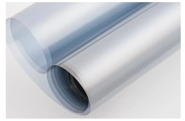
ITO (Indium Tin Oxide) thin films—transparent conductive oxide (TCO) composites comprising 90% In₂O₃ and 10% SnO₂—deliver high visible light transmittance and electrical conductivity. These properties underpin their ubiquitous industrial applications.
Industrial Applications of ITO Films
1.Photovoltaics
As transparent electrodes in heterojunction solar cells, ITO films ITO films can optimize the absorption of light and the transfer of charge, thereby enhancing the photoelectric conversion efficiency. In addition, the conductive and light-transmitting properties of ITO films also affect the conversion efficiency of perovskite solar cells and CIGS thin-film solar cells.
2.Display Panels
With 85–95% transmittance (comparable to glass) and low sheet resistance (R□: 15–100 Ω/sq), ITO serves as essential conductive layers for LCD/OLED displays and touchscreens in smartphones, tablets, and Electronic whiteboard.
3.Smart Windows
Smart windows leverage the high visible light transmittance and electrical conductivity of ITO films to adjust the light transmittance through the electric field, enabling achieve dynamic energy conservation and shading, and is applied to green energy-saving buildings and automotive glass.
4.Emerging Fields
At present, ITO films have emerged in multiple emerging industries such as AR/VR optical devices and medical detection sensors, and may play an important role in more new technological scenarios in the future.
Critical Parameters: Surface Roughness & Thickness
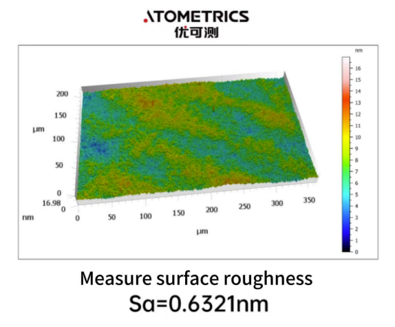
Surface Roughness Control
Surface roughness of ITO films critically impacts their electrical properties, optical performance, and device reliability. Excessive roughness (>3nm Ra) compromises carrier injection efficiency, induces undesirable light scattering, reduces light transmittance, and may cause pinhole defects or delamination in subsequent coatings (Such as: SiO₂ protective layers). The Atometrics AM-Series White Light Interferometer delivers precise ITO films roughness metrology with sub-nanometer scale accuracy and 400μm/s scanning speed, empowering manufacturers to optimize product performance while reducing costs and enhancing production yields.
Thickness
ITO film thickness critically governs their electrical properties, optical performance, and processing costs.
1.Sheet resistance varies with film thickness, necessitating precise thickness control tailored to application requirements;
2.Thickness determines optical path difference (OPD), with non-uniformity causing spectral shift in visible light transmittance curves;
3.Strategic thickness reduction within functional limits cuts material costs: Per 10nm decrease saves ≈15% indium consumption—particularly crucial for cost-sensitive large-area photovoltaic applications.
Atometrics AF-3000 series film thickness measuring instrument deliver sub-nanometer measure accuracy ITO film thickness supporting both offline and inline configurations with <0.5s/point measurement speed (including stage movement time).

Boardstone lntelligent(Shenzhen)Co.,Ltd.
14F,Building C Kaifa Plaza, 7006 Caitian Rd., Futian Dist. Shenzhen
Hotline:400 080 3885
Sales@atometrics.com.cn


