1. Widely Applied Microlens Arrays
A microlens is a fundamental micro-optical element. Through tailored design, it modulates incident light for diffusion, beam shaping, light homogenization, optical focusing, and integral imaging – enabling special functionalities unattainable with conventional optics components.
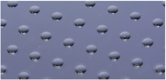
A Microlens Array (MLA) consists of tens to millions of micro-scale lenses (with micron-level apertures and relief depths) arranged in specific patterns. By adjusting lens geometry, focal length, array configuration, and fill factor, targeted optical performances are achieved. Based on beam modulation principles, MLAs are categorized into: Diffractive microlenses, Refractive microlenses, Hybrid (Fresnel) microlenses, Metalenses.
Source: MLA captured by Atometrics ultra-depth-of-field microscope
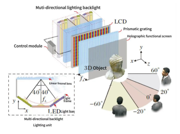
The application scope of MLAs ranges from fiber-optic coupling & beam conversion to laser homogenization, to the Coherent beam combining of same-wavelength lasers, and then to light-field 3D displays, computational imaging, projection illumination, high-sensitivity detection, optical security, wide-field imaging.
2. Client requirement : High-Speed Wafer-Scale MLA Metrology
Achieving Rapid & Accurate Full Inspection for Wafer-Scale MLAs
One of the global leader in materials, networking, an international brand, and laser technologies required full inspection of wafer-level MLAs at its Fuzhou facility. The client sought automated inspection systems that meeting the detection accuracy requirements, achieve a rapid improvement in detection efficiency.
MLA product characteristics determine the detection volume, each 8-inch wafer contains over 10,000 microlenses, measurement for evaluating the MLAs include Radius of Curvature (ROC), Surface roughness (Ra, Sa), Aspheric coefficient (K-value), Surface Profile Deviation (SPD), Lens Pitch and so on. The size of microlenses is at the micrometer level, while the surface roughness (such as Ra/Sa) is at the nanometer level.
For metrology systems, throughput and precision typically exhibit an inverse relationship. The critical challenge lies in performing full-wafer high-speed inspection of MLAs while maintaining micron-level accuracy – demanding not only hardware precision but also robust software algorithms and automation capabilities
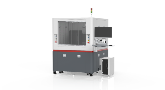
3. Atometrics Solution: Wafer 3D Automated Metrology System NX230 Series
10s/lens inspection cycle | 75% throughput increase
After rigorous benchmarking, the client adopted Atometrics' Wafer 3D automatic inspection equipment — NX230 series.
The NX230 series features a standard vacuum wafer chunk and an integrated metrology module comprising White light interferometer and Spectral Confocal Displacement Sensor. The white light interferometer is standardly equipped with high-precision piezoelectric ceramic (PZT) scanner (400μm/s max velocity). It is equipped with scientific CMOS (≤3,200Hz frame rate | 0.03nm vertical resolution). Combined with the industry's first SST+GAT algorithm and instantly complete the cloud processing (5M points/s acquisition).It is the first wafer 3D automatic measurement equipment in the industry with an accuracy of up to 0.03nm.
The system further enables fully automated inspection, incorporating auto-focusing, pattern recognition-based positioning, and programmed stage movement. It autonomously outputs measurement data for each lens, makes pass/fail (OK/NG) judgments, and performs grading, sorting, and thermal 3D map output, facilitating automated selection in downstream processes.
Measured parameters include Radius of Curvature (ROC), Numerical Aperture (NA), surface roughness (Ra/Sa, etc.), aspheric coefficient (K-value), and Surface Profile Deviation (SPD).
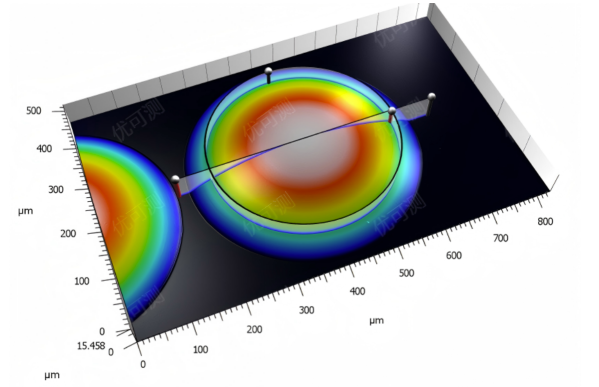
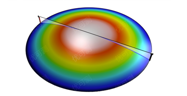
3D topography of microlens array (MLA)
Source: Scanning Imaging of Atometrics White Light Interferometer
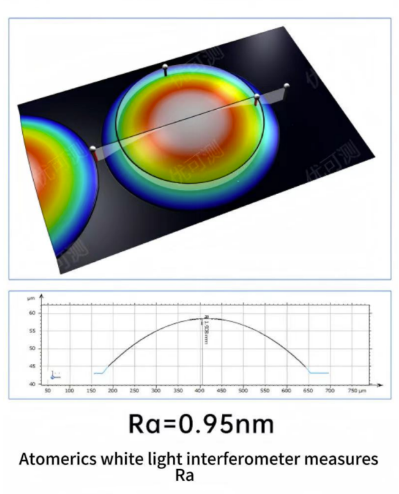
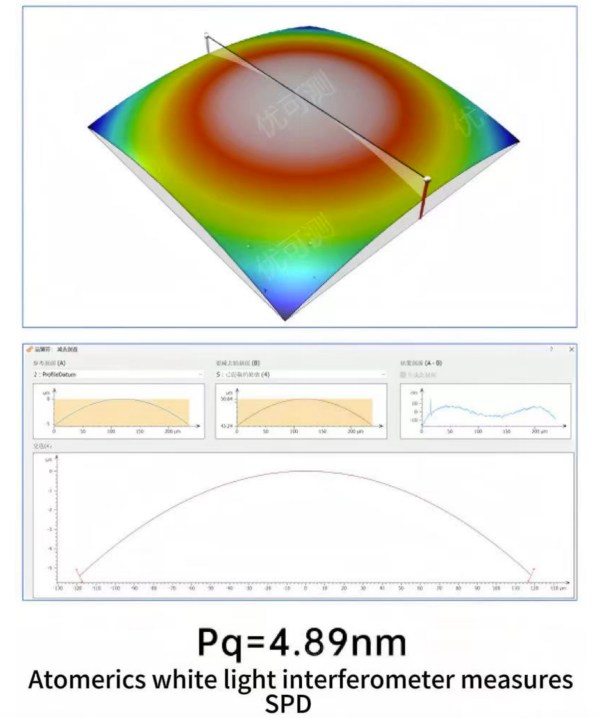
Measurement images generated by Atometrics equipment
This device can achieve a transition from "offline inspection" to "100% online inspection", achieving a 75% reduction in per-lens inspection time while maintaining micron-level accuracy, and the stability is within 0.2%. The detection capacity of a single device can be increased by more than six times (the working time of the equipment is calculated as 24 hours a day).
Furthermore, this equipment operates automatically, allowing single engineers to manage multiple systems, significantly boosting both shipment volumes and product quality for customers post-deployment.

Boardstone lntelligent(Shenzhen)Co.,Ltd.
6F Building C Kaifa Plaza,7006 Caitian Rd.,Futian Dist,Shenzhen
Hotline:400 080 3885
Sales@atometrics.com.cn
WhatsApp: +86 13316897904


