Wafer 3D Inspection WM Series
1. Principle of Wafer 3D Inspection WM Series
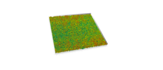
The Wafer 3D Inspection WM Series is based on the White Light Interferometry (WLI) principle. Interference fringes are generated when the optical path length from the light reflected off the object surface equals that from the internal reference mirror. A nanometer-level piezoelectric ceramic moves the optical path to acquire the phase difference of the interference fringes, which is converted into height (h) and resolved into a 3D height topography.
2. Applications of Wafer 3D Inspection WM Series
The Wafer 3D Inspection WM Series can measure:
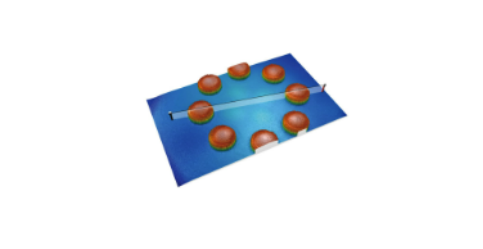
Wafer roughness (minimum measurable roughness 0.03 nm, compliant with ISO 25178 and ISO 4287 standards); Step height (maximum measurable step height 5000 µm, step height accuracy up to 0.3%); Wafer dicing/cutting depth; Dimensions related to photomasks/reticles;Dimensions related to bumping.
It is widely used in semiconductor manufacturing processes such as silicon ingot cutting, grinding & thinning, photomask/reticle fabrication, etching, dicing, marking, and bumping. It is also suitable for scenarios like consumables inspection and equipment experimentation.
3. Features and Advantages of Atometrics's Wafer 3D Inspection WM Series
Main Features:
Equipment Advantages:
Wafer 3D Metrology WPM Series
1. Principle of Wafer 3D Metrology WPM Series:
2. Applications of Wafer 3D Metrology WPM Series
The Wafer 3D Metrology WPM Series can measure:
Step height, film thickness, critical dimensions (CD), overlay accuracy, Warpage/Bow/Stress, Roughness, EBR (Edge Bead Removal), etc. In advanced packaging, it can measure the height, roughness, line width, line spacing, and line height of copper pillars, RDL (Redistribution Layer), UBM (Under Bump Metallization), bumps, etc. Can measure the profile of CMP (Chemical Mechanical Planarization/Polishing) processes.
It is widely used throughout the integrated circuit manufacturing flow, including IC design, wafer manufacturing stages, advanced packaging processes, and test processes. It covers steps such as lithography, etching, ion implantation, wafer dicing, electroplating, CMP, cleaning, and incoming/outgoing inspection.
3. Features and Advantages of Atometrics's Wafer 3D Metrology WPM Series:
Main Features:
Equipment Advantages:

Boardstone lntelligent(Shenzhen)Co.,Ltd.
6F Building C Kaifa Plaza,7006 Caitian Rd.,Futian Dist,Shenzhen
Hotline:400 080 3885
Sales@atometrics.com.cn
WhatsApp: +86 13316897904


