I. Core Functions
Based on spectral dispersion and confocal technology, the sensor enables multi-dimensional precision measurement. Specific functions include:
1. High-Precision 3D Topography and Dimensional Measurement
3D Surface Analysis: Generates 2048 measurement points per contour line to accurately depict object shapes. Capable of detecting geometric parameters such as thickness, step height, contour curvature, and offset. Achieves an X-direction resolution as low as 2 µm and a Z-axis repeatability accuracy as low as 0.05 µm, meeting micron-level and even sub-micron level measurement requirements.
Adaptable to different field-of-view requirements. The X-direction field-of-view covers 4.0 mm to 17 mm, with a maximum Z-direction depth of field reaching 5.5 mm, catering to measurement scenarios involving both minute structures and larger areas.
2. Multi-Material Compatibility Detection
Features strong anti-interference capability, effectively avoiding the impact of strong reflected light. Capable of achieving clear 3D imaging and precise measurement on various complex materials including transparent, semi-transparent, mirror-finish, highly reflective, and highly absorptive materials. Suitable for a wide range of industrial materials such as ceramics, metals, glass, and films.
3. Multi-Layer Intelligent Detection
Based on the optical detection method utilizing lateral chromatic aberration, a single scan can construct 2D and 3D data for multiple layers of transparent materials. It accurately covers details of each layer without requiring multiple adjustments, making it suitable for inter-layer analysis of structures like multi-layer films and transparent substrates.
4. Efficient Online Measurement
Maximum full depth-of-field measurement speed reaches 5000Hz (varies slightly between models). Combined with the feature of "offering both large and small fields of view with fast cycle times," it can adapt to online inspection needs on industrial production lines, enhancing inspection efficiency.
5. Integrated Software and Tool Support
Comes with built-in professional measurement software, featuring a simple and user-friendly debugging process. It is also equipped with a rich set of measurement tools to meet sample measurement requirements in different fields such as semiconductors and consumer electronics, lowering the operational barrier.
II. Core Advantages
1. Leading Precision and Powerful Measurement Performance
Excellent Key Parameter Performance: Achieves a minimum Z-axis repeatability accuracy of 0.05 µm and a minimum X-direction resolution of 2 µm, enabling nanometer-level precision measurement. This far exceeds traditional millimeter-level or ordinary micron-level sensors, making it suitable for high-precision scenarios like semiconductor chips and wafers.
High Data Acquisition Density: 2048 measurement points per contour line enable accurate capture of minute textures and defects, making measurement results more credible.
2. Wide Material Adaptability and Comprehensive Scenario Coverage
Breaks through the material limitations of traditional sensors. Compatible with complex materials like transparent, highly reflective, and highly absorptive ones without needing accessory changes, avoiding measurement errors or failures caused by material differences. Applicable to the inspection of various objects such as ceramic substrates, mobile phone screens, and PCB gold points.
3. Multi-Layer Detection + Efficient Measurement, Adaptable to Industrial Needs
The multi-layer detection function reduces repeated scanning steps, improving measurement efficiency for complex structures. The maximum measurement speed of 5000Hz, combined with an IP55 protection rating, meets the "fast cycle time, high stability" requirements for online inspection on production lines, balancing both precision and efficiency.
4. Solid Brand and Technical Foundation
Backed by Banshi Intelligent Technology (a National-Level "Specialized, Refined, Distinctive, and Innovative" Little Giant Enterprise), possessing a team of globally top scientists and seasoned engineers. Having received over 100 million RMB in investment from renowned institutions provides strong support for technological R&D and product quality.
Supported by a complete industrial layout (Shenzhen headquarters, Wuhan R&D center, etc.) and service system, offering full-process services such as sample measurement appointments and technical support, ensuring a good customer experience.
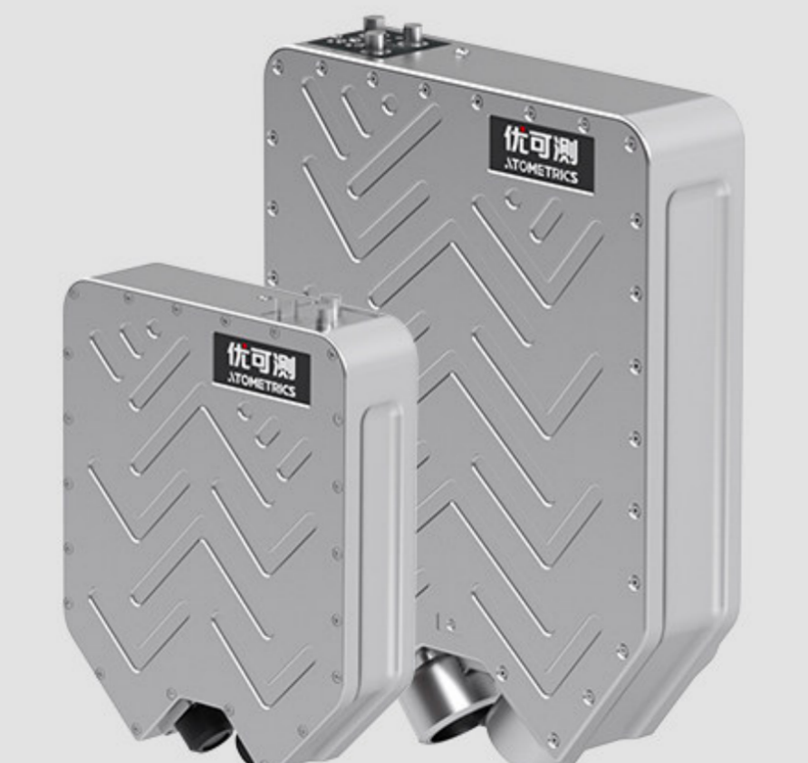
5. Diverse Specifications, Adaptable to Various Needs
The series includes four models: AS-7004, AS-7008, AS-7012, AS-7017, offering differentiated coverage in parameters such as field of view, depth of field, and measurement speed. They can be flexibly selected based on different measurement objects (e.g., small-sized chips, large-sized substrates).

Boardstone lntelligent(Shenzhen)Co.,Ltd.
6F Building C Kaifa Plaza,7006 Caitian Rd.,Futian Dist,Shenzhen
Hotline:400 080 3885
Sales@atometrics.com.cn
WhatsApp: +86 13316897904


