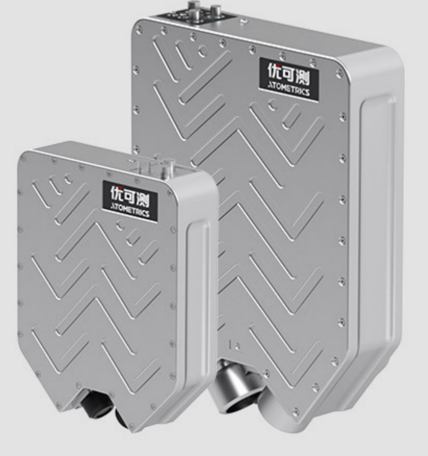
Principle of the 3D Line Spectral Sensor
The measurement principle of the AS-7000 series 3D line spectral confocal sensor is based on the combination of spectral dispersion and confocal technology. The core logic involves using spectral analysis to achieve precise capture of an object's three-dimensional information. The specific process is as follows:
Spectral Dispersion and Focal Plane Formation: The sensor first decomposes white light into a continuous wavelength spectrum. Light of different wavelengths focuses at specific vertical positions on the surface of the measured object, forming vertical focal planes corresponding to each wavelength.
Reflected / Transmitted Light Signal Acquisition: Utilizing the confocal principle, only specific wavelength light reflected or transmitted from the object's surface that is in focus passes through the optical system into the detector, while unfocused light is filtered out.
Data Analysis and 3D Reconstruction: By analyzing the information of the specific wavelength light captured by the detector and matching it to its corresponding focal position, the 3D topography, surface texture features, and spectral data of the object's surface are obtained. Simultaneously, each profile can generate 2048 measurement points, enabling precise depiction of the object's shape and achieving measurement precision at the micrometer to sub-micrometer level.
What Can the 3D Line Spectral Confocal Sensor Measure?
Through the principles of spectral dispersion and confocal imaging, the sensor can simultaneously capture an object's 3D topography, surface texture features, and spectral data. Based on 2048 measurement points per profile, it enables precise dimensional and morphological inspection. Core measurable indicators include:
Geometric Parameters: Such as thickness, step height, contour curvature, offset, etc.
Surface Characteristics: Such as texture details, micro-defects (e.g., integrity of PCB gold bumps)
Multi-layer Structure Data: 2D and 3D information of multiple layers in transparent/semi-transparent materials (e.g., multi-layer films, transparent substrates).
The document explicitly lists specific measurement cases for this sensor across multiple industries, covering the following areas:
|
Application Field |
Specific Measurement Object / Item |
Core Measurement Requirement |
|
Semiconductor Industry |
Semiconductor chips, wafer-related structures |
High-precision dimensional inspection, surface defect identification, inter-layer structure verification, suitable for micrometer/sub-micrometer level requirements |
|
Electronics Manufacturing |
PCB (Printed Circuit Board) gold bumps |
Morphological integrity, positional accuracy, and micro-dimension measurement of gold bumps, avoiding errors caused by reflection interference |
|
Consumer Electronics |
Mobile phone screen edge contours, curvature |
Accurate depiction of screen curved surface morphology, ensuring assembly fit and appearance precision |
|
Precision Manufacturing |
Ceramic substrate coatings |
Measurement of coating thickness, step height (height difference between areas), suitable for non-homogeneous materials like ceramics |
The sensor features strong anti-interference capability and compatibility with multiple materials, enabling effective measurement of various complex materials, including:
Transparent / semi-transparent materials (e.g., glass, films).
Highly reflective / mirror-like materials (e.g., metal components, optical elements).
Highly light-absorbent materials (e.g., certain polymer materials, dark coatings).
Hard / brittle materials (e.g., ceramics, semiconductor wafers).
Combining its "abundant measurement tools" and "suitability for industrial online inspection" (fast cycle time, high precision), it can also be extended to:
Precision structure measurement of 5G communication devices (e.g., contour and dimensions of antenna components).
3D dimension and defect inspection of packaging substrates.
Thickness and inter-layer structure analysis of film materials (e.g., collaborative scenarios with AH-3000 series film thickness measurement instruments).
Application Industries for the 3D Line Spectral Confocal Sensor
The AS-7000 series 3D line spectral confocal sensor, with its core advantages of high precision, multi-material compatibility, multi-layer detection, and fast measurement, is widely used in multiple industrial fields with high demands for precision measurement, as detailed below:
As one of the core application fields, the sensor meets the precision measurement requirements at the micrometer to sub-micrometer level in semiconductor manufacturing, primarily applied in:
3D surface analysis, surface defect, and critical dimension inspection of semiconductor chips.
Three-dimensional metrology of wafers, inter-layer structure verification, and micro-offset detection (e.g., Die Shift).
3D dimension, defect, and assembly accuracy measurement of packaging substrates (suitable for collaborative scenarios with devices like the Elite Pro series packaging substrate inspection equipment).
Addressing the "high precision, high aesthetics" manufacturing requirements of consumer electronics, the sensor enables precision inspection of key components:
Mobile phone screens: Precise measurement of edge contours and surface curvature, ensuring screen assembly fit and appearance precision.
Other precision electronic components: Such as surface texture, dimensional tolerance, and assembly step height inspection of camera modules, optical elements, etc., compatible with complex materials like transparent and mirror surfaces.
Focusing on precision inspection of printed circuit boards (PCB) and related electronic components, solving measurement challenges posed by highly reflective materials:
PCB gold bump inspection: Accurately identifies the morphological integrity, positional accuracy, and micro-dimensions of gold bumps, effectively avoiding interference from metal reflections on measurement results.
Pin size, solder joint quality, and surface defect inspection of electronic components.
Covers production inspection scenarios for various high-precision components and materials, suitable for multi-material and complex structure measurement needs:
Ceramic substrates: Precise measurement of coating thickness and inter-layer step height (height difference between areas).
Other precision components: Such as 3D topography, surface roughness metrology, and multi-layer structure analysis of optical films, metal precision parts, etc.
Leveraging its high-precision measurement capability for micro-structures, it adapts to the precision manufacturing and inspection needs of 5G communication devices:
5G antenna components: Contour dimension, assembly gap, and surface defect inspection.
Packaging structure, pin accuracy, and inter-layer connection status measurement of communication modules.

Boardstone lntelligent(Shenzhen)Co.,Ltd.
6F Building C Kaifa Plaza,7006 Caitian Rd.,Futian Dist,Shenzhen
Hotline:400 080 3885
Sales@atometrics.com.cn
WhatsApp: +86 13316897904


