In semiconductor manufacturing, Particle Defects refer to tiny particles or impurities formed on the surface or within the silicon wafer. These defects can originate from various factors such as impure raw materials, equipment wear, environmental contamination, or operational errors. Particle defects compromise the structural integrity of devices, leading to electrical failures like short circuits or open circuits, and severely impact the long-term reliability of the devices. They are a critical quality issue that requires strict control in semiconductor manufacturing.
How Particle Defects Are Generated
The generation mechanisms of particle defects are complex and can be broadly categorized into physical and chemical factors. Physical factors include mechanical stress and temperature variations. During manufacturing processes, handling, processing, and thermal treatment of silicon wafers can cause mechanical stress accumulation. If the stress exceeds the material's limit, it can lead to surface cracks or material spalling. Rapid temperature changes generating thermal stress may also cause cracks or particle detachment.
Chemical factors primarily involve chemical reactions and corrosion. Chemical reagents and gases used in manufacturing may react under specific conditions, producing undesired byproducts or impurities that adhere to the wafer surface, forming defects. Additionally, corrosive effects can lead to surface roughness or pits. Beyond physical and chemical factors, common sources of particle defects also include impurities in raw materials, internal equipment contamination, environmental dust, and human operational errors.
Common Types of Particle Defects
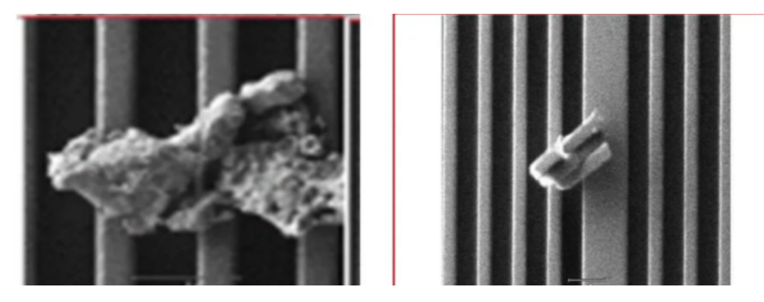
Based on their location and characteristics, particle defects can be classified into two main categories: Surface Particles and In-Film Particles. Surface Particles refer to particles from the process environment landing on the wafer surface, often appearing as clusters with sharp edges. In-Film Particles occur when particles fall onto the wafer during thin film formation and become embedded within the subsequently deposited film layer.
Considering specific causes and morphology, common particle defects include dust particles, metal residues, and photoresist residues. Dust particles primarily result from airborne dust in the production environment; metal residues typically originate from equipment wear or metal impurities in chemical reagents; photoresist residues stem from incomplete removal of photoresist during lithography processes. Other defect types include bubbles, cracks, scratches, etc., each with different formation mechanisms and impacts.
Impact of Particle Defects on Semiconductors
Particle defects have a direct negative impact on the electrical performance of semiconductor devices. Dust particles or metal residues may form unintended conductive paths within the device, causing abnormal current flow and leading to short circuits or open circuits. In highly miniaturized and integrated devices where circuit spacing is extremely small, the risk of particle defects causing short circuits increases significantly. Photoresist residues can obstruct current flow, affect circuit pattern accuracy, and even compromise circuit integrity.
Defects also severely undermine device reliability. Particle contamination may adhere to critical areas such as circuit nodes or transistor gates, causing short circuits, open circuits, or performance instability, with problems potentially worsening over time. Structural defects like cracks and spalling, often related to uneven internal stress, temperature fluctuations, or mechanical shock, can lead to circuit breaks or open circuits. These defects not only cause device performance degradation but may also result in complete failure, with particularly severe consequences in critical applications such as aerospace and medical equipment.
How to Detect and Control Particle Defects
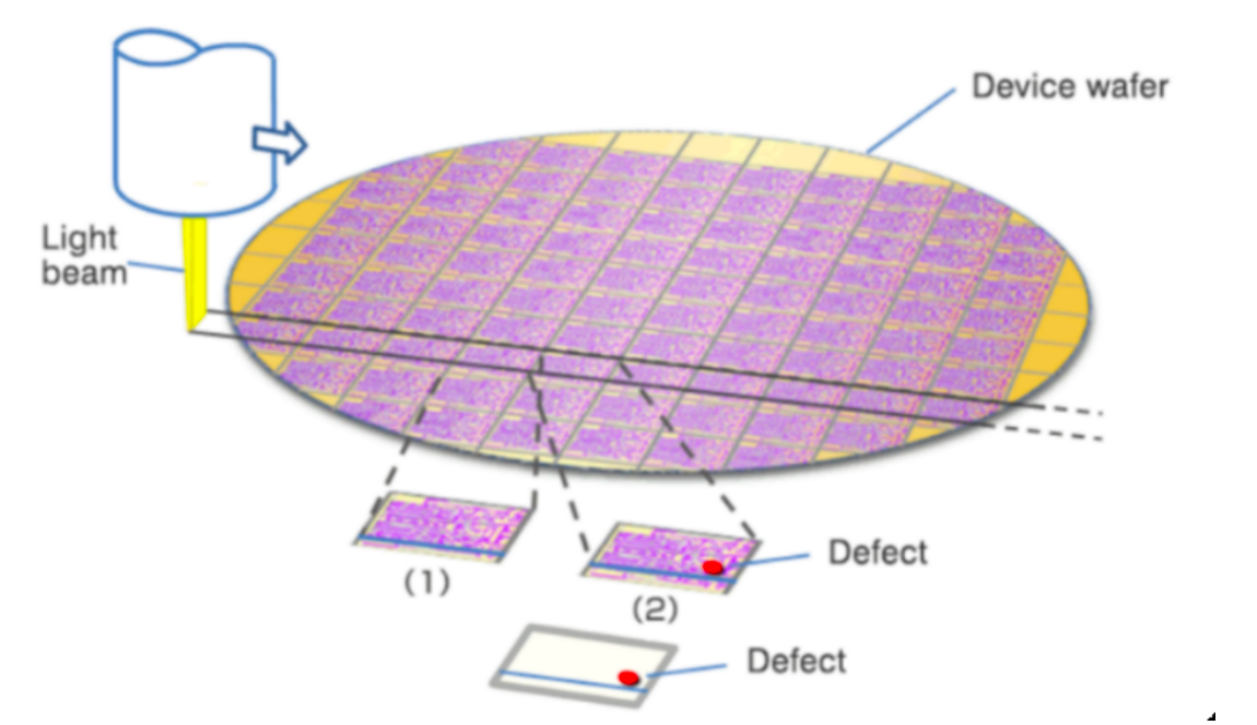
Detection of particle defects primarily relies on high-precision microscopy techniques. The Scanning Electron Microscope (SEM), with its high resolution and imaging capabilities, is a core tool for defect detection, capable of revealing the morphology, size, and distribution of tiny particles. The White Light Interferometer, utilizing the principle of White Light Interference to map 3D surface topography, offers extremely high precision in nanoscale defect detection. Optical microscopes are used for rapid screening of larger defects.
To control particle defects, multifaceted measures are required. Regarding raw materials and processes, material purity should be improved, and parameters such as etch rate, deposition thickness, temperature, and pressure must be precisely controlled. For equipment and environment, it is essential to select high-precision, high-stability equipment, perform regular maintenance and calibration, and strictly control environmental conditions like cleanliness, temperature, and humidity. Human factors cannot be overlooked. Operator skills should be enhanced through training, operational practices standardized, and process monitoring and management strengthened. By comprehensively analyzing defect morphology and composition to identify the contamination source and promptly addressing it, the occurrence rate of defects can be effectively reduced.

Boardstone lntelligent(Shenzhen)Co.,Ltd.
6F Building C Kaifa Plaza,7006 Caitian Rd.,Futian Dist,Shenzhen
Hotline:400 080 3885
Sales@atometrics.com.cn
WhatsApp: +86 13316897904


