In recent years, with the continuous development of electronic technology, the input power requirements for chips have become increasingly higher. High-power products necessitate good heat dissipation performance. For electronic devices, as temperature rises, device lifespan decreases accordingly; for every 10°C increase in temperature, the effective lifespan is reduced by 30% to 50%. Ceramic substrates, owing to their excellent thermal conductivity, heat resistance, corrosion resistance, high insulation, radiation resistance, high stability, and low thermal expansion, are seeing growing application demand in fields such as electronic devices, optoelectronic devices, and microwave devices. Consequently, the precision requirements for ceramic substrates are also becoming increasingly stringent.
Therefore, during the manufacturing of ceramic substrates, it is essential to measure parameters such as surface roughness, flatness, thickness, line width, line spacing, copper thickness, height difference, and warpage. Selecting inspection instruments with appropriate accuracy, suitable inspection speed, and sufficiently high performance and cost-effectiveness is particularly important at this stage.
So, what are the advantages of ceramic substrates? What are the inspection requirements? And what kind of measuring instruments should be selected for inspection?
Overview and Classification of Ceramic Substrates
Ceramic materials refer to a class of inorganic non-metallic materials formed by shaping and high-temperature sintering of natural or synthetic compounds.
A substrate is a material with specific properties and functions, used for supporting and protecting chips, facilitating heat dissipation, and connecting to the underlying circuit board.
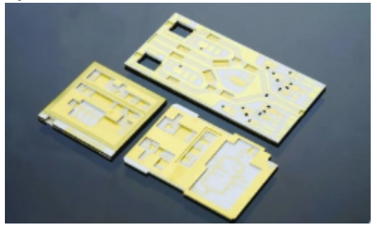
A ceramic substrate is an electronic packaging material prepared using a ceramic material as the base body through specific process methods. It is a special type of PCB substrate, characterized by good thermal conductivity, high insulation, high stability, and a relatively high dielectric constant. Therefore, it is widely used in electronic packaging, optoelectronic devices, and other fields.
Ceramic substrates are primarily classified by material type into oxide ceramic substrates, nitride ceramic substrates, and carbide ceramic substrates. Among them, oxide ceramic substrates mainly include aluminum oxide (Alumina), beryllium oxide (Beryllia), and zirconium oxide (Zirconia). Nitride ceramic substrates mainly include aluminum nitride (AlN) and silicon nitride (Si3N4). Carbide ceramic substrates mainly include silicon carbide (SiC) and boron carbide (B4C).
Ceramic substrates are classified by structure mainly into planar ceramic substrates and multilayer ceramic substrates. Classified by process, they mainly include HTCC (High-Temperature Co-fired Ceramic), LTCC (Low-Temperature Co-fired Ceramic), DPC (Direct Plated Copper), DBC (Direct Bonded Copper), TPC (Thick Film Printing), TFC (Thin Film), AMB (Active Metal Brazing), and LAM (Laser Activated Metallization).
Differences Between Ceramic Substrates and Ordinary PCB Boards
Material: Ordinary PCB boards use organic materials, while ceramic substrates use inorganic non-metallic materials such as oxides, nitrides, and carbides.
Performance and Application: Ordinary PCB boards have a wide range of applications, while ceramic substrates, due to their excellent thermal conductivity, are mostly used in products with high heat dissipation requirements, high power, and those prone to heating.
Advantages and Disadvantages of Ceramic Substrates
Advantages
Disadvantages
Ceramic substrates are mostly single-sided or double-sided. If made into multilayer boards, the scrap rate is high, and the process requirements and costs are also very high. In contrast, ordinary PCB boards can be made into multilayer boards (dozens of layers are possible) and can be produced in large sizes that are less fragile.
Application Scope of Ceramic Substrates
Due to their good thermal conductivity, high insulation, and high stability, ceramic substrates are mostly used in industries with high power and significant heat dissipation requirements. For example:
High-Power Electronic Modules
Third-Generation Semiconductors (e.g., SiC)
Inspection Requirements for Ceramic Substrates
Different types of ceramic substrates have specific requirements for surface roughness, polishing precision, thickness, flatness, line width, line spacing, copper thickness, and machining tolerances for circuit boards.
1. Surface Roughness Measurement
The roughness of the copper-clad surface on a ceramic substrate affects circuits with fine pitch and high-density interconnects. Polishing the ceramic substrate reduces the peak-to-valley amplitude on the substrate surface, thereby enabling the use of very thin metal layers. Thinner resistive layers increase the sheet resistance of the material. Therefore, precise measurement of the surface roughness of ceramic substrates is necessary.
2. Flatness Measurement and Warpage
The flatness of a ceramic substrate affects the adhesion of the surface copper cladding, consequently influencing the substrate's voltage, resistance, and ultimately the product's safety and performance. Thus, precise measurement of the flatness of ceramic substrates is required during manufacturing.
3. Thickness Dimension
Thicker ceramic substrates offer better strength and pressure resistance, but poorer thermal conductivity. Conversely, thinner substrates have relatively lower strength and pressure resistance but stronger thermal conductivity. Therefore, measuring the thickness of ceramic substrates is essential to control the required thickness for different application scenarios.
4. Line Width, Line Spacing, Copper Thickness
Variations in the trace width on ceramic substrates affect impedance changes, which can cause signal reflection and impact signal integrity. Therefore, inspection of line width, line spacing, and copper thickness on ceramic substrates is required.
5. R-angle (Edge Radius)
Some ceramic substrates require gold plating. During the manufacturing process, it is necessary to measure and control the edge collapse (or smear) to manage the material cost of the gold plating.

Boardstone lntelligent(Shenzhen)Co.,Ltd.
6F Building C Kaifa Plaza,7006 Caitian Rd.,Futian Dist,Shenzhen
Hotline:400 080 3885
Sales@atometrics.com.cn
WhatsApp: +86 13316897904


