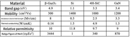
Gallium Oxide (Ga₂O₃), an emerging fourth-generation semiconductor material, demonstrates significant potential for high-voltage power devices, deep-ultraviolet photoelectric devices, and electronics for extreme environments due to its ultra-wide bandgap (~4.9 eV), high breakdown field strength (8 MV/cm), and excellent Baliga Figure of Merit (approximately 10 times that of SiC and 4 times that of GaN). Compared to third-generation semiconductors like Silicon Carbide (SiC) and Gallium Nitride (GaN), Ga₂O₃ possesses a wider bandgap, higher theoretical breakdown voltage, and enables the growth of large-size single crystals via melt methods, significantly reducing substrate preparation costs. Furthermore, Ga₂O₃ materials maintain stable electrical properties even in high-temperature and high-radiation environments, making them ideal candidates for next-generation high-efficiency power electronic devices.
The cost structure of the Ga₂O₃ industry chain is similar to that of the third-generation semiconductor SiC, influenced by material properties and preparation processes. Costs are predominantly concentrated in the substrate (e.g., iridium-based methods) and epitaxy segments, collectively accounting for over 80%, while device manufacturing constitutes only 10%~20%.
The global Ga₂O₃ industry landscape shows notable regional variations: Japan maintains a comprehensive leading advantage, having established a complete substrate-epitaxy-device industry chain. FLOSFIA in Japan has pioneered the commercial mass production of amorphous Ga₂O₃ power devices, while collaboration between Tohoku University and C&A Corporation on an iridium-free process holds promise for reducing substrate costs by 90%, injecting strong momentum into the industry chain development. The United States has formed a research and development system covering all segments, with particularly outstanding achievements in the device field, continuously pushing performance boundaries through novel structural designs and process optimization [1]. In contrast, China's Ga₂O₃ industry remains primarily in a research institution-led development stage. Although the wide-bandgap semiconductor trend has spurred several startups, industrialization progress is relatively slow. Currently, only small-batch provision of Ga₂O₃ substrates is possible, with industrialization in the epitaxy and device segments nearly non-existent.
Ga₂O₃ Epitaxial Preparation Methods
Ga₂O₃ devices are fabricated on epitaxial thin films; therefore, high-quality, low-defect Ga₂O₃ epitaxy is crucial for producing high-performance devices. The mainstream methods for preparing Ga₂O₃ epitaxial thin films to date include: Halide Vapor Phase Epitaxy (HVPE), Molecular Beam Epitaxy (MBE), Mist Chemical Vapor Deposition (Mist-CVD), and Metalorganic Chemical Vapor Deposition (MOCVD). A comparison of these different Ga₂O₃ epitaxial technologies is shown in the figure below:
media/image2.png
Halide Vapor Phase Epitaxy (HVPE)
HVPE is a high-speed epitaxial technique based on halide vapor phase reactions, using GaClₓ (generated from the reaction of HCl with metallic Ga) and O₂/H₂O as precursors to deposit β-Ga₂O₃ films on substrates at 800–1100°C. Its core advantages include ultra-high growth rates (10–200 μm/h) and carbon-free high purity, with background carrier concentrations potentially as low as 10¹⁵ cm⁻³, while supporting a wide range of n-type doping (10¹⁵–10²⁰ cm⁻³), perfectly matching the requirements of high-voltage power devices for thick epitaxial layers (>10 μm) and low doping. However, HVPE-grown films face challenges such as surface roughness (requiring polishing or THVPE process optimization) and relatively high defect density, and achieving atomic-level control of heterointerfaces is difficult. Currently, institutions like Japan's NICT have achieved the preparation of 6-inch epitaxial wafers, with 4-inch products passing device verification. THVPE technology has further reduced surface roughness to <1 nm [2]. HVPE is regarded as ideal for Ga₂O₃ vertical power devices but requires complementation with MOCVD/MBE technologies to cover the entire industry chain needs.
Molecular Beam Epitaxy (MBE)
MBE is a technique conducted in an ultra-high vacuum environment, involving the precise control of Gallium (Ga) beam flux and oxygen plasma/O₃ molecular beams to react and deposit Ga₂O₃ films on the substrate surface. Its hallmark feature is atomic-level control capability, enabling precise δ-Si doping (accuracy ±1 monolayer) and sharp control of heterointerface transitions (<0.5 nm transition layer). Traditional MBE is limited by the desorption effect of Ga₂O sub-oxides, typically resulting in growth rates <300 nm/h (e.g., with oxygen plasma source). However, sub-oxide MBE (S-MBE), by directly supplying Ga₂O molecular beams, can increase the growth rate to 1 μm/h (at 525°C) while maintaining surface roughness <2 nm (for 1 μm films) and precise silicon doping control (5×10¹⁶–10¹⁹ cm⁻³) [3]. Research indicates that the growth rate on β-Ga₂O₃ (010) substrates is over 30% higher than on other crystal planes [4]. The US AFRL team, using ozone (O₃) instead of oxygen plasma, achieved a growth rate of 130 nm/h at 650°C [5], while low-temperature MBE (using composite sources) on sapphire substrates can further reduce the growth temperature [6]. MBE is currently primarily used in scientific research for developing high-end devices (e.g., quantum wells, superlattices), but its low speed (<0.1 μm/h) and complex, expensive equipment costs limit its industrial application.
Mist Chemical Vapor Deposition (Mist-CVD)
Mist-CVD is an emerging low-cost technique for preparing Ga₂O₃ thin films. It utilizes ultrasonic nebulization (~2.4 MHz) to convert gallium oxide precursor solutions (e.g., GaCl₃, Ga(acac)₃) into micron-sized aerosols, which are transported by carrier gas (N₂/O₂) to deposit Ga₂O₃ films under atmospheric pressure at 400-700°C. The advantages of this technology include equipment costs only 10%~20% of traditional CVD, process temperatures 300~500°C lower than MOCVD, and the use of water-soluble precursors, offering both safety and environmental benefits. Currently, this technique has been successfully applied to the preparation of α-Ga₂O₃ and κ(ε)-Ga₂O₃ films. Japan's FLOSFIA pioneered the mass production of 4-inch α-Ga₂O₃ films and developed the world's first 1700V/1A-class Schottky barrier diodes based on this [7]. However, the industrialization of Mist-CVD still faces challenges such as poor uniformity control for large-size (>4 inch) film deposition, the introduction of various unintentional dopants during growth, and the poor thermal stability of the metastable α-Ga₂O₃ phase.
Metalorganic Chemical Vapor Deposition (MOCVD)
As the most mature industrialized epitaxial technology in the compound semiconductor field, MOCVD enables large-area deposition of Ga₂O₃ films with high-precision thickness control, while also allowing adjustment of film composition and doping concentration by controlling gas flow rates, offering strong process scalability. It has become the preferred growth technology for the industrialization of Ga₂O₃ epitaxy. The technical principle involves the thermal decomposition reaction of metalorganic gallium sources (e.g., TEGa, TMGa) and oxygen sources (O₂, N₂O, or H₂O) on the high-temperature substrate surface to achieve the epitaxial growth of Ga₂O₃.
Traditional MOCVD growth of Ga₂O₃ epitaxy faced the bottleneck of low growth rates (<0.5 μm/h), primarily due to premature precursor consumption caused by gas-phase pre-reactions. Recently, through reactor structure innovations, such as using close-coupled showerhead (CIS) or coupled dual-showerhead (CCS-MOCVD) designs to separately deliver the gallium and oxygen sources [8], the growth rate has been successfully increased to 10 μm/h (at 900°C), while maintaining high crystalline quality and smooth surface morphology of the films.
Current research progress shows that the performance of β-Ga₂O₃ films grown by MOCVD has reached industry-leading levels. The US Kyma Technologies team, using N₂O as the oxygen source, reduced the unintentional doping concentration to the 10¹⁴ cm⁻³ range [9]; Chinese scientists achieved a room-temperature electron mobility of 184 cm²/(V·s) (carrier concentration 2.5×10¹⁶ cm⁻³) on β-Ga₂O₃ (010) substrates, approaching the theoretical limit [10]. In terms of industrialization, Japan's Novel Crystal Technology has achieved mass production of 4-inch MOCVD epitaxial wafers with stable growth rates of 3-5 μm/h and defect density <10⁶ cm⁻², suitable for 600-1200V power devices.
Ga₂O₃ Epitaxy
Ga₂O₃ epitaxy includes two technical routes: homoepitaxy and heteroepitaxy. For homoepitaxy, the substrate is typically β-Ga₂O₃, and the crystal plane must be selected based on the specific epitaxial method [11]. Heteroepitaxial substrate materials generally include sapphire, GaN, and Strontium Titanate (SrTiO₃). Due to lattice mismatch and thermal expansion coefficient mismatch in heteroepitaxy, buffer layer technology is often required to improve the quality of the epitaxial film, although its crystalline quality is usually inferior to homoepitaxy.
Homoepitaxy
Commonly used substrate planes for homoepitaxy include the cleavage planes (100), (001) and non-cleavage planes (010), (101) of β-Ga₂O₃. Different epitaxial techniques have specific requirements for crystal orientation. For instance, in MBE, the deposition rate on the (010) plane is significantly higher than on the (100) plane, with differences up to 10-fold [12], whereas in MOCVD processes, the substrate orientation has a relatively smaller impact on deposition rate [13]. For homoepitaxy on β-Ga₂O₃ (100) substrates, despite perfect lattice matching between the substrate and epitaxial layer, defects such as stacking faults and twins still occur during growth, limiting carrier mobility improvement. Employing a step-flow growth mode can effectively suppress defect formation, enabling the preparation of defect-free Ga₂O₃ films by controlling growth kinetics. Research shows that substrate off-cut treatment can effectively achieve step-flow growth mode for β-Ga₂O₃ (100) homoepitaxy. Schewski's team found [14] that when using MOCVD, a 6° off-cut angle is the critical value for achieving step-flow growth, resulting in defect-free films; whereas with off-cut angles less than 6°, growth proceeds via a 2D island mode, accompanied by defects like stacking faults and twins. Subsequently, Bin's team made significant breakthroughs through process optimization [15], achieving step-flow on Ga₂O₃ (100) substrates with different off-cut angles (2°, 4°, 6°), increasing the epitaxial rate from 1.6 nm/min to 4.3 nm/min, and raising the room-temperature electron mobility to 131 cm²/(V·s).
Heteroepitaxy
Given the low thermal conductivity of β-Ga₂O₃ (only 0.14 W/(cm·K)), which presents heat dissipation limitations, researchers have attempted direct heteroepitaxial growth on substrates with high thermal conductivity. Common substrates for heteroepitaxy include sapphire, GaN, and SrTiO₃. Schewski's team [16] found that c-plane sapphire stabilizes the α-Ga₂O₃ phase but introduces mismatch dislocations. Akaiwa's team [17] significantly improved the crystalline quality and mobility of α-Ga₂O₃ by introducing an annealed buffer layer. Compared to sapphire, GaN offers better thermal conductivity and optical properties. Cao's team [18] prepared β-Ga₂O₃ epitaxy on GaN(0001) via MOCVD followed by annealing, discovering that adjusting the annealing temperature could induce phase transformation from amorphous → single crystal → polycrystal. The preparation of Ga₂O₃ epitaxy on SrTiO₃ substrates has also been studied. Wang's team [19] used MOCVD to epitaxially grow β-Ga₂O₃ films on SrTiO₃(100) substrates, followed by annealing at different temperatures. They found that annealing at 1000°C yielded single-crystal β-Ga₂O₃ with a visible light transmittance of 75%.
White Light Interferometer for Rapid Substrate Surface Roughness Measurement
Currently, some domestic Ga₂O₃ substrate manufacturers utilize Atometrics White Light Interferometers to perform 3D topography acquisition and measurement of Ga₂O₃ substrate surfaces, as well as to measure substrate surface roughness.
The Atometrics White Light Interferometer comes standard with high-precision piezoelectric ceramics (PZT), a maximum scanning speed of 400 μm/s, and is equipped with a high-sensitivity, high-pixel CMOS camera capable of up to 3200 Hz scan frame rate. Combined with the industry-first SST+GAT algorithm, it can instantly acquire up to 5 million point clouds, achieving a sample measurement repeatability deviation of 0.006 nm. In comparative tests with Atomic Force Microscopes (AFM), the measurement accuracy corresponds precisely.

In efficiency comparisons, the surface roughness measurement of a single point on a Ga₂O₃ substrate sample using an Atomic Force Microscope required nearly 20 minutes, whereas using the Atometrics White Light Interferometer generates a test report in approximately 3 seconds, significantly improving sample measurement efficiency and saving valuable time for R&D departments.

Boardstone lntelligent(Shenzhen)Co.,Ltd.
6F Building C Kaifa Plaza,7006 Caitian Rd.,Futian Dist,Shenzhen
Hotline:400 080 3885
Sales@atometrics.com.cn
WhatsApp: +86 13316897904


