Specialist in high-precision measuring instruments: The measurement principle of the Automated Non-Contact Thickness Measurement System (APS Series) is primarily based on the Chromatic Confocal Principle and Spectral Interferometry Principle, combined with a dual-probe (upper and lower) structural design to achieve high-precision non-contact surface measurement. The details are as follows:
I. Core Measurement Principles
1. Chromatic Confocal Principle
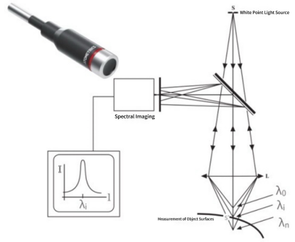
This principle utilizes the correspondence between the wavelength of light and the focal distance to achieve thickness and height measurements. The specific process is:
· Light Source Emission and Transmission: The equipment is equipped with a "white point light source". The light is transmitted via optical fibers and lens groups to illuminate the surface of the object under test.
· Confocal Filtering: After light of different wavelengths irradiates the object, only the light focused precisely on the object's surface meets the "confocal condition" (i.e., the light rays converge accurately at a single point).
· Signal Reception and Analysis: The reflected light satisfying the confocal condition is transmitted to the "CMOS spectral imaging unit". Through spectral analysis and algorithmic computation, it is ultimately converted into the true physical height information of the object, thereby deriving parameters such as thickness.
2. Spectral Interferometry Principle
media/image2.png
This principle is designed according to the optical characteristics of specific materials like silicon wafers, making it suitable for high-precision thickness detection. Its core characteristics include:
· Wavelength Adaptability: Utilizes the optical transparency of silicon wafers within the 1100nm wavelength range, employing an IMS5420 interferometer for precise thickness detection. At this wavelength, both undoped and doped silicon wafers possess sufficient transparency.
· Measurement Range: Capable of detecting wafers with thicknesses up to 1.05 mm, with a measurement range for air gaps even reaching up to 4 mm.
II. Structural Design and Principle Synergy
To enhance measurement efficiency and parameter coverage, the equipment adopts a dual-probe chromatic confocal opposing design, further optimizing the practical application of the principles:
· Dual-Probe Layout: Upper and lower probes are symmetrically arranged, with the sample placed between them. A single test can simultaneously acquire comprehensive geometric parameters including Thickness, TTV (Total Thickness Variation), Bow, Warp, TIR (Total Indicated Runout), and LTV (Local Thickness Variation).
· Industry Adaptability: This dual-probe design complies with SEMI (Semiconductor Equipment and Materials International) standards, granting it broad applicability in fields such as semiconductors, MEMS (Micro-Electro-Mechanical Systems), and compound epitaxy.
III. Error Elimination and Accuracy Assurance
Specialized optimization schemes are integrated into the principle application to address environmental and equipment errors during the measurement process:
· For warp measurement, deviations caused by stage vibration and the virtual reference plane are eliminated through the "upper-lower opposite measurement" technique, significantly improving the measurement accuracy for Bow and Warp parameters.
· Combined with high-precision hardware (e.g., sensors with 1nm resolution, anti-vibration systems), it ensures that the principles deliver micron-level or even sub-micron level accuracy in practical measurements.

Boardstone lntelligent(Shenzhen)Co.,Ltd.
6F Building C Kaifa Plaza,7006 Caitian Rd.,Futian Dist,Shenzhen
Hotline:400 080 3885
Sales@atometrics.com.cn
WhatsApp: +86 13316897904


