Introduction to Chip Decap
Chip Decap, short for Decapsulation, also referred to as opening or un-capping, is a technical process of locally treating a fully packaged integrated circuit (IC) chip. It involves removing the external packaging material through physical or chemical means to expose internal structures such as the die, bond wires, and pads.
The core objective of this step is to prepare the chip for subsequent failure analysis, fault localization, electrical testing, or microscopic observation without damaging its internal components and functionality. Chip decapsulation is applicable to various packaging types, including BGA, QFP, QFN, SOP, ceramic packages, and metal packages, making it a key procedure in semiconductor failure analysis and reverse engineering.
Purpose of Chip Decap
Chip decapsulation serves several core purposes in the semiconductor industry. Firstly, it is primarily used for failure analysis, helping technicians locate physical defects inside the chip, such as short circuits, open circuits, corrosion, or interlayer delamination. The decapsulation process can also be used for reliability verification, inspecting the quality of packaging processes, such as whether bond wires are broken or whether delamination exists in the packaging material.
Furthermore, in reverse engineering, decapsulation can be employed to obtain design information such as circuit layout and process node of the chip, which is used for patent infringement verification or chip authenticity identification.
Decapsulation technology is also an important means of evaluating packaging quality. By observing details such as solder joints and connecting wires, it ensures that the packaging process meets standard requirements, thereby improving the overall reliability and performance of the chip.
In terms of importance, chip decapsulation serves as a bridge between chip packaging and in-depth analysis. It not only provides the physical foundation for failure mode analysis, chemical analysis, and fault localization but also offers key data support for improving chip manufacturing processes. Through decapsulation, analysts can visually inspect the internal structure and, combined with electrical testing and microscopy techniques, accurately diagnose the root cause of failures, thereby optimizing design and production processes.
Main Classification of Chip Decap
Depending on the packaging material and analysis requirements, chip decapsulation is mainly divided into three methods: chemical decapsulation, mechanical decapsulation, and laser decapsulation. Each method has its applicable scenarios and technical characteristics.
1. Chemical Decapsulation
Chemical decapsulation is currently the most mainstream method, particularly suitable for plastic-encapsulated chips (such as epoxy resin packages). Its principle involves using strong acid reagents (such as fuming nitric acid or concentrated sulfuric acid) to dissolve the packaging resin through heating or chemical reactions, thereby exposing the chip's internal structure. This method offers high processing efficiency and is suitable for batch operations. However, the acid concentration and reaction time must be strictly controlled to avoid corroding metal bond wires or introducing contamination. Chemical decapsulation is typically performed in a fume hood, and operators must wear acid-resistant equipment to ensure safety.
2. Mechanical Decapsulation
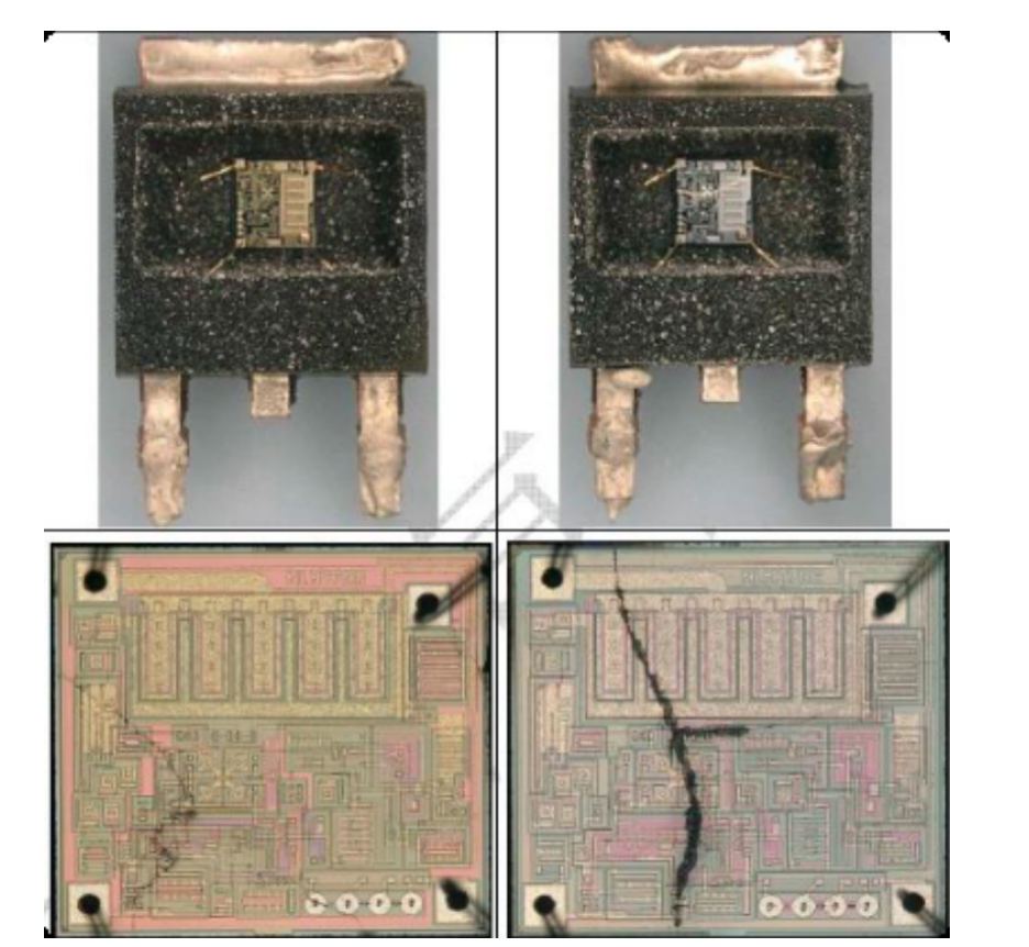
Mechanical decapsulation primarily targets chemically resistant materials such as ceramic or metal packages. It involves removing the package body through physical grinding, cutting, or polishing. This method is simple to operate and has relatively low equipment costs, but it is prone to causing mechanical damage to the chip's surface circuitry and is time-consuming. Mechanical decapsulation is often used in scenarios where the lead frame or package housing needs to be preserved. It requires fine operation under a microscope, gradually removing material until the internal structure is exposed.
3. Laser Decapsulation
Laser decapsulation is a high-precision, non-contact advanced technology that uses a high-energy laser beam (such as a UV laser) to vaporize the packaging material layer by layer. This method is suitable for advanced packaging forms (such as Flip-Chip, 3D IC) or stress-sensitive devices. It enables localized decapsulation with micron-level precision without introducing mechanical stress or chemical contamination. However, laser decapsulation equipment is costly, requires specialized operators, and improper energy settings may cause damage to metal layers.
Specialist in high-precision measuring instruments, such as white light interferometers, often employ laser decapsulation in conjunction with non-contact surface measurement techniques to perform detailed topographical analysis of exposed structures without physical contact, ensuring high accuracy and preserving delicate features.
Chip Decap Operational Procedure
Taking the most commonly used chemical decapsulation as an example, its operational procedure can be divided into four stages: preliminary preparation, sample handling, decapsulation execution, and post-cleaning. The entire process must be conducted under safety protections.
During the preliminary preparation stage, operators must wear personal protective equipment such as acid-resistant masks, gloves, and goggles, and perform operations within a fume hood. Emergency equipment such as eyewash stations, shower devices, and acid neutralizers should also be prepared.
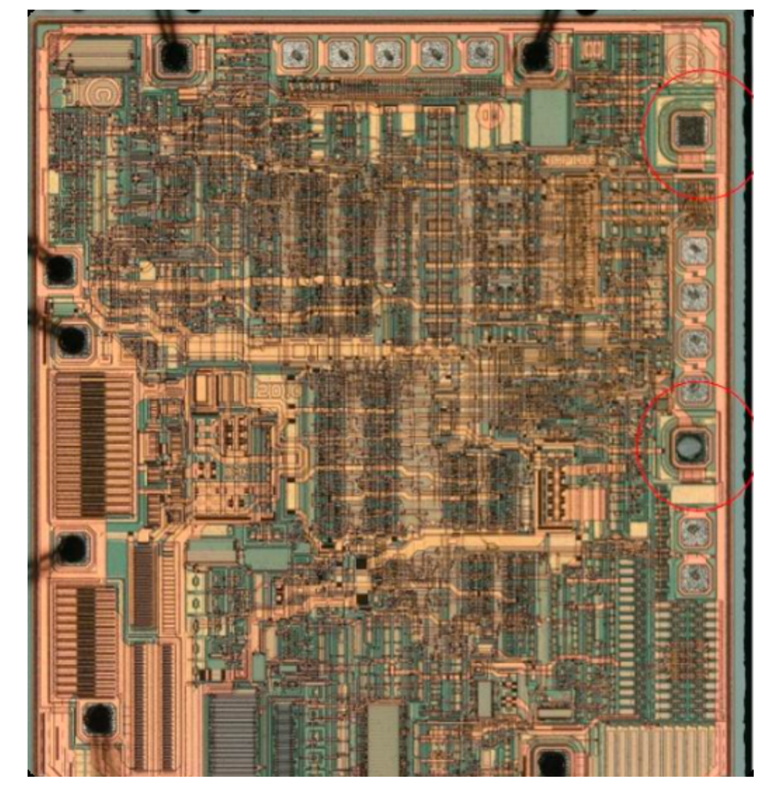
In the sample handling stage, the chip model and packaging type are first confirmed. Preliminary judgment of the internal structure is made through X-ray to determine the decapsulation plan. The chip is then cleaned and fixed using special fixtures to protect the pins and bottom, exposing only the area to be decapsulated.
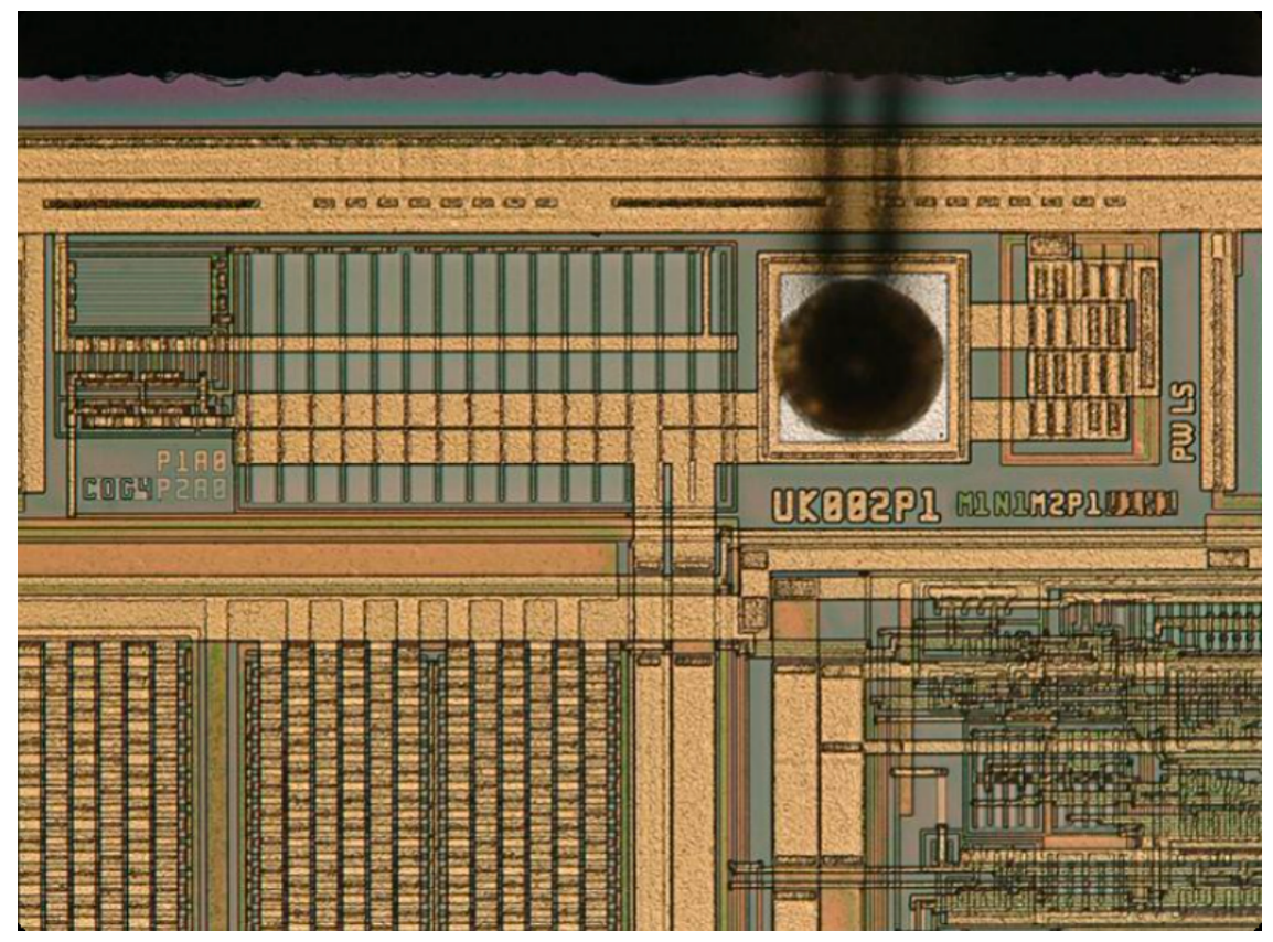
The decapsulation execution stage primarily employs the acid-drop method or the spraying method. The acid-drop method involves using a precision pump to drip fuming nitric acid onto the chip surface, heating it to 60°C–80°C to accelerate the reaction, and monitoring the corrosion progress in real-time under a microscope. Once the bond wires or die surface are exposed, acid dripping is immediately stopped, and the chip is rinsed with copious amounts of deionized water to neutralize residual acid. The spraying method involves uniformly spraying acid through a nozzle, which is suitable for decapsulating larger areas.
After the reaction is terminated, ultrasonic cleaning and nitrogen blow-drying are required to ensure the chip surface is free from contamination.
Mechanical and laser decapsulation procedures have their own characteristics. Mechanical decapsulation involves gradually removing material with a grinder or cutting tool, requiring repeated microscopic inspection of progress. Laser decapsulation, controlled by computer programming of the laser path, enables automated operation with high precision but at higher equipment costs. Regardless of the method, microscopic inspection or electrical testing is required after decapsulation to verify the effectiveness of the procedure and proceed with subsequent analysis.
Typical Application Scenarios of Chip Decap
In terms of applications, chip decapsulation is widely used for failure analysis in fields such as automotive electronics and consumer electronics. For example, if an MCU chip fails during high-temperature testing, laser decapsulation might reveal broken bond wires, thereby identifying a packaging process defect. In intellectual property protection, decapsulation technology is used to compare the circuit layouts of competitor chips to verify patent infringement. Simultaneously, decapsulation is an important means for packaging quality verification and material analysis, contributing to improved chip reliability and yield.
Chip Decap is a precision operation that integrates chemical, mechanical, and optical technologies, serving as a fundamental step in failure analysis and reverse engineering. By selecting appropriate decapsulation methods, strictly following operational procedures, and enhancing safety protections, the internal structure of chips can be effectively exposed, providing critical support for fault diagnosis and process optimization. In the future, with technological iterations, the decapsulation process will become more precise, safer, and more efficient, further aiding the quality improvement and innovation of the semiconductor industry.

Boardstone lntelligent(Shenzhen)Co.,Ltd.
6F Building C Kaifa Plaza,7006 Caitian Rd.,Futian Dist,Shenzhen
Hotline:400 080 3885
Sales@atometrics.com.cn
WhatsApp: +86 13316897904


