Case Study: Wafer Thickness Inspection
An electronics research institute required automated Total Thickness Variation (TTV) measurement on production lines with ≤1μm accuracy to screen defective units. Atometrics addressed this need through tailored testing and solution design:
1. Point Measurement: Engineers measured thickness at 6 randomly selected points on the wafer and obtain the thickness of each point.
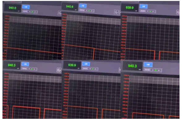
2. Automated Simulation: Stage movement emulated real-time production-line scanning to test the thickness variation of the wafer.
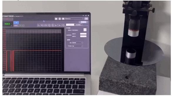
To meet customers' requirements for carriers in terms of different sizes, materials, and thicknesses, Atometrics has developed customized carriers tailored to their needs, ensuring the stability of inspections. The surface of the carriers is customized into vacuum adsorption carriers based on the characteristics of customers' products, guaranteeing high precision when the products are in a flat state. In addition, Atometrics provides customers with overall machine frame design. For customers' special measurement requirements, Atometrics also has certain development and coordination capabilities in script editing, and offers after-sales debugging and software development assistance services.
After receiving the sample test results and the scheme design, the customer said, "We didn't expect that the point spectroscopy measurement effect of Atometrics is so good, and the overall machine frame design also fully meets our needs. Finally, we can realize automated measurement on the production line!"
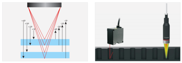
Measurement Principle: Atometrics Spectral Confocal Displacement Sensor
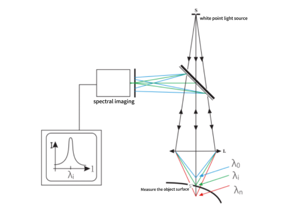
A white point light source emits through optical fiber and lens assemblies onto the target surface. Polychromatic light focuses at varying heights, creating a measurement range. Only wavelengths focused precisely on the surface reflect back through the dispersive lens assembly, where they separate into monochromatic components projected onto a CMOS spectral imaging array. Ultimately, determines target object surface height through analyzing the wavelength of the reflected light.
Three Key Advantages of Atometrics Spectral Confocal Displacement Sensor
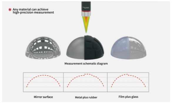
1. Material Agnosticism & Stability:
Achieves high-precision measurement on any material—including transparent substrates—via stable multi-layer surface recognition. Coaxial chromatic confocal technology enables dead-angle-free measurement even in narrow cavities.
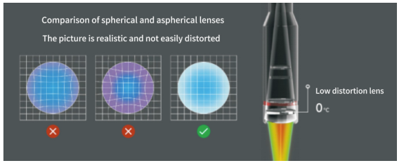
2. Thermally Stable High Precision:
Unlike laser displacement sensors prone to thermal deformation-induced drift, Atometrics's sensor measurement unit is designed with only a lens structure inside, which does not generate heat. Coupled with a low-distortion lens group, it can achieve ideal high-precision measurement.
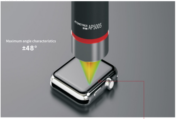
3. Large-Angle Capability (±48°):
Atometrics's sensors’ maximum Angle characteristic reaches ±48°, making it easy to measure radians.

Boardstone lntelligent(Shenzhen)Co.,Ltd.
14F,Building C Kaifa Plaza, 7006 Caitian Rd., Futian Dist. Shenzhen
Hotline:400 080 3885
Sales@atometrics.com.cn


