Gallium Oxide Process Breakthrough! Poised for Large-Scale Applications
In recent years, gallium oxide (Ga₂O₃), as an "ultra-wide bandgap semiconductor" material, has garnered sustained attention. From an industry classification perspective, ultra-wide bandgap semiconductors belong to the "fourth-generation semiconductors." Compared to third-generation semiconductors like silicon carbide (SiC) and gallium nitride (GaN), gallium oxide boasts a bandgap of 4.9 eV, surpassing SiC's 3.2 eV and GaN's 3.39 eV.
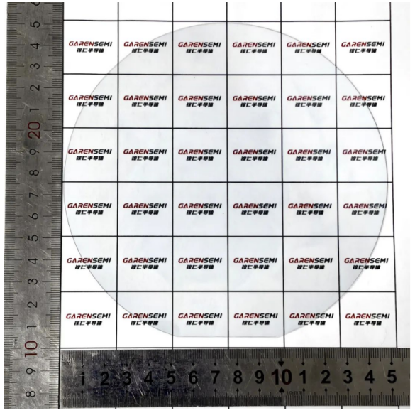
Source: Gallium Oxide Substrate Sample
A wider bandgap means electrons require more energy to transition from the valence band to the conduction band. This endows gallium oxide-based power devices with higher operating currents and voltages, lower on-resistance, smaller device sizes, and higher conversion efficiency, giving them significant advantages for manufacturing high-performance power devices. Industry experts predict gallium oxide will see widespread adoption in automotive and electrical equipment applications between 2025 and 2030.

Garensemi Leads with 6-Inch Gallium Oxide Substrate Sales
Zhejiang-based renowned semiconductor company "Hangzhou Garensemi Co., Ltd.", leveraging the State Key Laboratory of Silicon and Advanced Semiconductor Materials at Zhejiang University, the Zhejiang University Hangzhou International Innovation Center, and the Zhejiang Provincial Key Laboratory of Wide Bandgap Semiconductor Materials and Devices, has successfully pioneered a novel casting method (CM) for gallium oxide single crystal growth. This breakthrough enabled the launch of 6-inch CM single crystal substrates, making Garensemi the first to achieve 6-inch sales. Concurrently, Garensemi completed domestic verification of its 4-inch Vertical Bridgman (VB) method gallium oxide crystal growth equipment and process package, now fully available for sale.
Surface Roughness Metrology and 3D Topography Requirements
In their R&D work, Garensemi's development department requires inspection equipment to perform 3D topography acquisition and measurement of gallium oxide substrate surfaces, as well as measure substrate surface roughness.
Atometrics White Light Solution Boosts Inspection Efficiency to Seconds
After multiple rounds of evaluation and comparison, the R&D team ultimately adopted the Atometrics AM7000 Series White Light Interferometer.
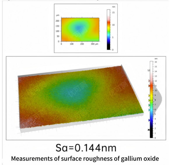
The Atometrics White Light Interferometer AM Series features a standard high-precision piezoelectric ceramic (PZT) stage with a maximum scanning speed of 400 μm/s. It is equipped with a high-sensitivity, high-pixel CMOS camera capable of scanning rates up to 3200 Hz. Combined with the industry-first SST+GAT algorithm, it instantly captures up to 5 million data points. The repeatability deviation for sample measurements reaches 0.006 nm. In comparative tests with Atomic Force Microscopy (AFM), its measurement accuracy showed precise correspondence.
In efficiency comparisons, measuring the surface roughness of a single point on a gallium oxide substrate sample using AFM took nearly 20 minutes. In contrast, the Atometrics White Light Interferometer AM Series generated the test report in approximately 3 seconds. This significantly enhances sample measurement throughput, freeing up invaluable time for the R&D department."

Boardstone lntelligent(Shenzhen)Co.,Ltd.
14F,Building C Kaifa Plaza, 7006 Caitian Rd., Futian Dist. Shenzhen
Hotline:400 080 3885
Sales@atometrics.com.cn


