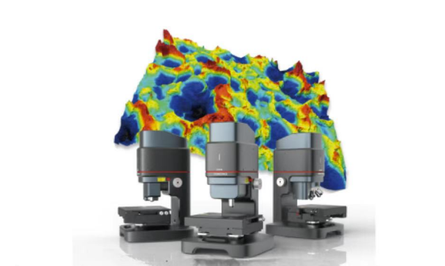
The quality of wafer substrates is crucial for the performance of infrared detector chips. Atometrics White Light Interferometers enable high-precision measurement of sub-nanometer surface roughness, nanometer-scale step heights, overall flatness, and microscopic 3D topography of these wafer substrates.
From the discovery of infrared radiation in the 18th century to the invention of infrared detectors in the 19th century, the technology has evolved significantly. Today, with ongoing process updates and iterations, infrared detectors are rapidly advancing towards multi-band capability, large array formats, high resolution, and low-cost mass production.
Today, Dr. Atometrics takes you to explore the science behind infrared detection.
I. What is Infrared Light?
Infrared light is a type of electromagnetic wave, typically with wavelengths ranging from 0.75 μm to 1000 μm.
It exhibits strong thermal effects and significant radiative capacity. The warmth we feel from sunlight is primarily due to solar infrared radiation.
However, as infrared light is invisible to the human eye, we cannot observe it directly.
II. Applications of Infrared Detection
In daily life and industrial production, the properties of infrared light are frequently utilized for detection. Infrared detectors can capture radiant energy and convert it into electrical signals or images. Their applications are extensive, spanning sectors such as medical, industrial, security, military, and meteorology.
1. Infrared Detection + Temperature:
Examples: Infrared thermometers, industrial infrared sensors, chemical plant leak detection.
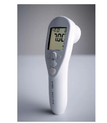
Infrared Thermometer
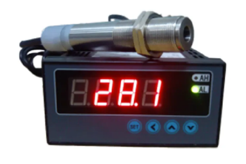
Industrial Temperature Sensor
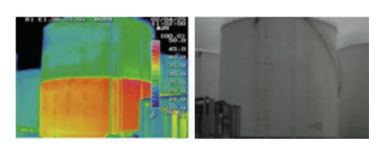
Leak Detection
2. Infrared Detection + Camera:
Examples: Thermal imaging cameras, night vision devices.
Thermal Imaging Camera

Night Vision Device
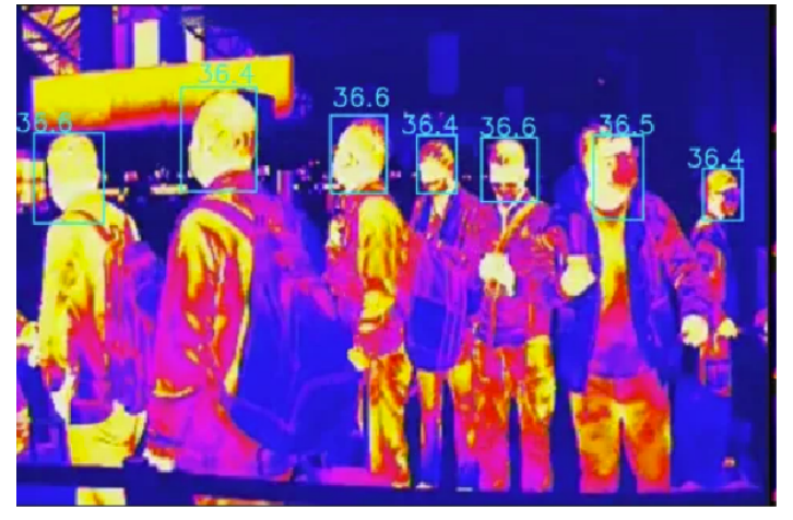
3. Infrared Detection + Tracking Systems:
Examples: Missile tracking systems.
Missile Tracking System
III. Infrared Detection Chips
The infrared detection chip is the core unit of an infrared detector. Due to the specialized applications of infrared detectors in military fields, infrared chip technology was subject to long-term international embargoes. After decades of development, domestic Chinese infrared chips have made significant progress in both R&D and production, successfully overcoming these technological barriers and largely achieving domestic substitution.

Infrared Detector Chip
Infrared detection chips are typically manufactured using materials such as Gallium Antimonide (GaSb), Indium Antimonide (InSb), Cadmium Zinc Telluride (CdZnTe), or Mercury Cadmium Telluride (HgCdTe) as wafer substrates. They are produced through a series of wafer-level packaging processes including etching, passivation, metallization, and packaging.
Wafer Substrate
In this process:
The surface roughness of the wafer substrate affects photosensitivity, resolution, and sensitivity.
The etched step height impacts electron transport efficiency.
The flatness influences final packaging yield.
Therefore, stringent control over the surface roughness, step height, and overall flatness of the wafer substrate is essential.
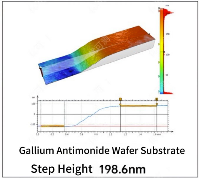
Atometrics White Light Interferometer AM-7000 Series:
Performs high-precision measurement of sub-nanometer surface roughness, nanometer-scale step heights, and overall flatness measurement of wafer substrates. It is already assisting several leading domestic infrared wafer substrate and infrared chip manufacturers in achieving R&D breakthroughs and improving production processes.
To learn more about inspection cases, or if you have any precision inspection requirements,
Atometrics engineers will prioritize providing you with the optimal inspection solution!

Boardstone lntelligent(Shenzhen)Co.,Ltd.
6F Building C Kaifa Plaza,7006 Caitian Rd.,Futian Dist,Shenzhen
Hotline:400 080 3885
Sales@atometrics.com.cn
WhatsApp: +86 13316897904


