Raw Material Required for Chip Manufacturing: Silicon
With the continuous advancement of technology, intelligence and informatization have become indispensable parts of our lives. As the foundation of the electronic information industry, the importance of chips is self-evident. In the chip manufacturing process, silicon raw material plays a crucial role. Manufacturing chips requires silicon, one of the fundamental raw materials. Silicon is not only abundant on Earth but also offers superior environmental benefits due to its non-toxic nature.
Semiconductor integrated circuits refer to electronic components that integrate numerous elements on a single chip, used for processing and storing various functions. The "Wafer" is the foundation for manufacturing integrated circuits. Most chips are made from silicon extracted from sand, grown into a single-crystal ingot, and then sliced into thin, round pieces of appropriate thickness.
Ingot Growth
First, sand is heated to separate carbon monoxide and silicon, a process repeated until ultra-high-purity Electronic Grade Silicon (EG-Si) is obtained. The high-purity silicon is melted into a liquid, which then solidifies into a single-crystal solid form called an "ingot." This is the first step in semiconductor manufacturing.
Ingot growth is the core step in forming single-crystal silicon, determining the crystal quality and electrical properties of the wafer. Manufacturing methods include the Czochralski Method and the Float-Zone Method, both involving the controlled growth of silicon crystals from a high-purity silicon melt.
Czochralski Method (CZ Method)
High-purity polycrystalline silicon (purity >99.9999999%, i.e., 9N grade) is placed in a quartz crucible and heated to 1420°C under an inert gas atmosphere (e.g., argon) until molten.
A single-crystal silicon seed crystal is dipped into the molten silicon. By slowly rotating and pulling it upward (speed approx. 1-3 mm/min) while precisely controlling the temperature gradient, the molten silicon solidifies along the crystal lattice direction of the seed, forming a single-crystal silicon ingot. Suitable for producing large-diameter ingots (mainstream 300mm, future 450mm). The ingot may contain trace amounts of oxygen (from the quartz crucible) and carbon impurities, requiring subsequent annealing treatment.
Float-Zone Method (FZ Method)
A high-frequency coil is used to locally heat a polycrystalline silicon rod, creating a molten zone. By moving the coil, the molten zone travels from the bottom to the top. Impurities are driven to the ends due to the segregation effect, and the impurity-concentrated parts are ultimately cut off. Offers high purity (extremely low oxygen content), suitable for manufacturing high-performance devices like power semiconductors and detectors. Higher cost, smaller ingot diameter (typically ≤200mm).
Wafer Slicing
After the previous step, a diamond saw is used to cut off both ends of the ingot, which is then sliced into thin pieces of a specific thickness. The diameter of the sliced ingot determines the wafer size. Larger, thinner wafers can be divided into more usable units, helping to reduce production costs. After slicing, a "flat zone" or "notch" is added to the slices as a reference for setting the processing direction in subsequent steps. The most common wafer slicing techniques: blade cutting, laser cutting, and plasma cutting.
Blade Cutting, also known as mechanical dicing, is the most widely used wafer slicing technique. It uses a high-speed rotating blade (often coated with abrasives like diamond particles) to cut the semiconductor wafer and separate individual chips. The blade is mounted on a dicing saw, which precisely controls the cut position and depth to ensure accurate chip separation according to design specifications.
● Advantages: Versatility and compatibility with various semiconductor materials, including silicon, germanium, and gallium arsenide. It is a mature and cost-effective technology capable of handling wafers of various sizes and thicknesses relatively easily.
● Limitations: Mainly evident when dicing smaller, more densely packed chips. The mechanical stress induced during cutting can cause chipping, cracking, or deformation of the fine internal structures of the chips.
Laser Cutting is a non-contact surface measurement wafer slicing technique primarily using a focused laser beam to separate individual chips on a semiconductor wafer. A high-energy laser beam is directed onto the wafer surface, initiating a process of ablation/pyrolysis, thereby vaporizing or removing wafer material along predetermined cutting lines (streets). Laser types used include Ultraviolet (UV), Infrared (IR), and Femtosecond lasers. UV lasers are widely used due to their high photon energy, enabling precise cold ablation with minimal Heat-Affected Zone (HAZ), reducing thermal damage to the wafer and surrounding chips. IR lasers are suitable for thicker wafers due to their deeper material penetration. Femtosecond lasers produce extremely short light pulses, enabling highly efficient and precise material removal with almost no heat conduction.
● Advantages: High precision and accuracy. The laser beam can be focused to a very small spot, allowing for cutting complex patterns and leaving minimal kerf between chips. This is beneficial for advanced semiconductor devices with ever-shrinking dimensions.
● Limitations: The process can be slower and more expensive for high-volume production.
Plasma Cutting, also known as plasma etching or dry etching, is another advanced wafer slicing technique primarily using Reactive Ion Etching (RIE) or Deep Reactive Ion Etching (DRIE) to separate individual chips on a semiconductor wafer.
This technique uses plasma (an ionized gas composed of charged particles) to chemically remove wafer material along predetermined cutting lines. During plasma cutting, the semiconductor wafer is placed in a vacuum chamber, and a controlled mixture of reactive gases is introduced. An electric field is then applied to generate a plasma from the gas mixture, creating a high concentration of reactive ions and radicals. These active species interact with the wafer material, selectively removing it through a combination of chemical reactions and physical sputtering. The etch rate and selectivity can be controlled by adjusting plasma parameters (e.g., gas composition, pressure, power).
● Advantages: Reduced mechanical stress on the wafer and chips. Being a non-contact method involving no mechanical force, the risk of chipping, cracking, or deformation is lower. High precision and accuracy.
● Limitations: The process is complex and time-consuming, especially for thick wafers or materials with high etch resistance.
Wafer Polishing
The thin slices obtained through the above cutting process are called "bare wafers" or unprocessed "raw wafers." Their surfaces are uneven and unsuitable for directly printing circuit patterns. Therefore, surface imperfections are first removed through grinding and chemical etching processes. Subsequently, polishing creates a smooth surface. Finally, cleaning removes residual contaminants, resulting in a finished wafer with a pristine surface.
Chemical Mechanical Polishing (CMP)
● Rough Polishing (Lapping): Uses alumina or diamond abrasives to remove the cutting damage layer (approx. 20-50 μm), reducing surface roughness to about 1 μm.
● Precision Polishing (CMP):
- Polishing Slurry: Alkaline solution (pH 10-11) containing nano-sized silica (SiO₂) or cerium oxide (CeO₂) particles.
- Polishing Pad: Porous polyurethane material, providing a synergistic effect of mechanical friction and chemical corrosion.
- Final surface roughness metrology (Ra) <0.5 nm, local flatness (TTV) <1 μm.
Cleaning
● Uses SC1 (NH₄OH+H₂O₂+H₂O) and SC2 (HCl+H₂O₂+H₂O) solutions to remove particles and metal contamination.
● Rinsing with Ultrapure Water (resistivity >18 MΩ·cm) followed by nitrogen drying.
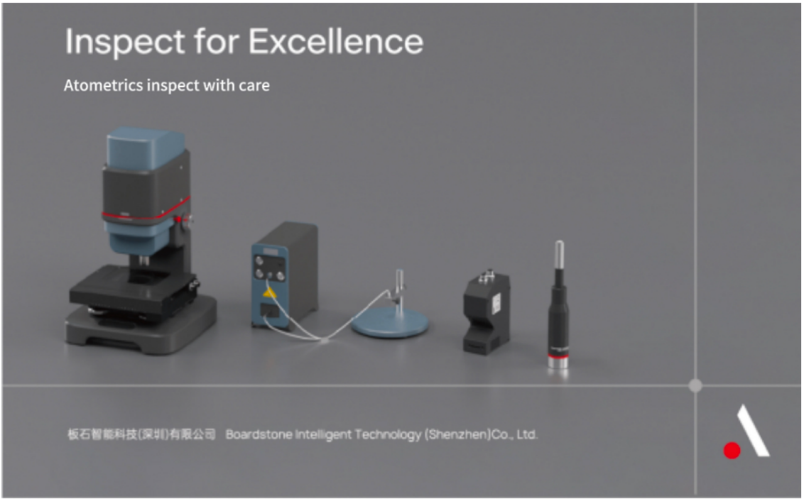
Inspection
● Surface Defects: Laser scattering inspection systems (e.g., KLA-Tencor Surfscan) identify micro-scratches and particles.
● Resistivity Uniformity: Four-point probe method measures silicon wafer resistivity distribution.
Wafer preparation is the cornerstone of semiconductor manufacturing. Its process precision directly impacts chip performance and yield. From the perfect growth of the single-crystal silicon ingot to the realization of a nano-level polished surface, each step requires the integration of cutting-edge technologies from materials science, precision mechanics, and chemical engineering.


Boardstone lntelligent(Shenzhen)Co.,Ltd.
6F Building C Kaifa Plaza,7006 Caitian Rd.,Futian Dist,Shenzhen
Hotline:400 080 3885
Sales@atometrics.com.cn
WhatsApp: +86 13316897904


