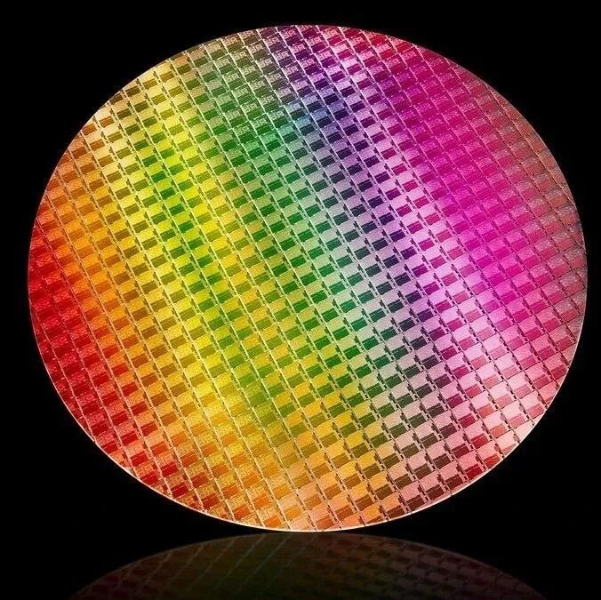
As semiconductor manufacturing processes advance toward the 3nm and 2nm nodes, the precision required for wafer processing has reached the micrometer or even nanometer scale. Producing a qualified wafer—from raw material to surface processing—poses significant challenges to manufacturing capabilities. For the increasingly common ultra-thin wafers, mechanical brittleness increases sharply once the thickness drops below 50 μm. When dealing with wafers made from third-generation semiconductor materials like SiC or GaN—which are characterized by high hardness and processing difficulty—inspection standards become even more rigorous, and precision requirements rise accordingly.
Diamond Wafers:
Inspection Challenges for Next-Generation Heat Spreaders
Compared to traditional silicon or glass wafers, diamond wafers offer exceptional thermal conductivity, mechanical strength, hardness, and electrical insulation. Their ultra-high thermal conductivity, in particular, aligns perfectly with the demands of modern, highly stacked chip architectures. When used as heat spreaders, diamond wafers must be bonded to GaN or silicon wafers. During the bonding process, controlling "warp" and "bow" is critical, as these parameters directly determine the quality of the bond interface; additionally, the wafer's Total Thickness Variation (TTV) impacts the precision of the bonded assembly.
Pain Points in Traditional Inspection
Inspection Challenges for Next-Generation Heat Spreaders
In the past, many factories employed contact-based thickness measurement methods for these types of hard, brittle wafers; these involved pressing a probe against the wafer surface to obtain thickness data at specific points. However, such methods have significant drawbacks:
Risk of sample damage: Mechanical contact from the probe not only risks scratching the diamond wafer surface, but the pressure exerted—particularly on ultra-thin diamond wafers—can also cause the wafer to fracture, resulting in the loss of raw materials.
Inadequate efficiency and data completeness: Single-point measurement is inefficient; inspecting a single wafer often takes ten minutes and yields data for only a limited number of points. Consequently, it is impossible to fully assess the uniformity of thickness and topography across the entire wafer surface, making it difficult to meet the quality control requirements of advanced manufacturing processes.
Atometrics Wafer Metrology Solutions
High Precision, High Speed, and Customization
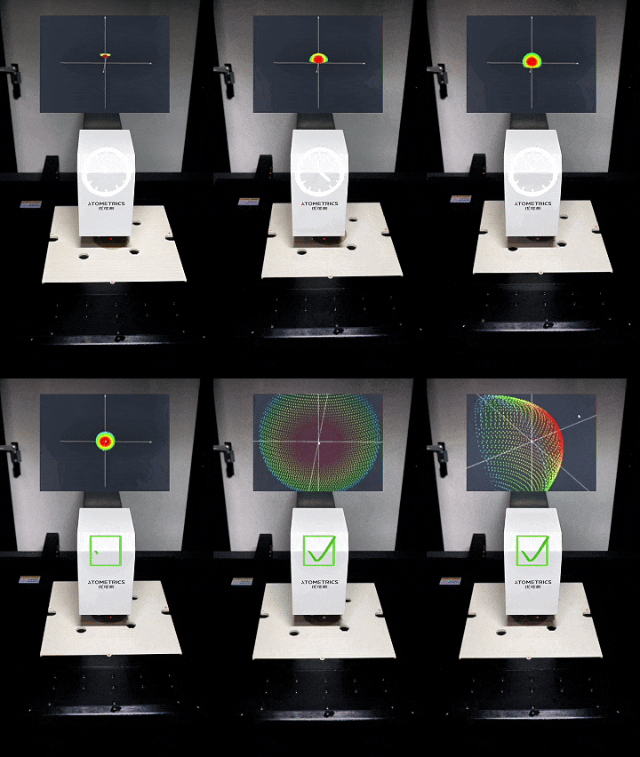
We recently received a request from a client to measure the TTV (Total Thickness Variation), Warp, and Bow of 3-inch polycrystalline diamond wafers, with a precision requirement at the sub-micron level. The project utilized the U-Precise APS series—a fully automated, non-contact thickness measurement system—yielding the following results:
Non-contact opposed-point spectral technology completely eliminates damage:
We employ opposed-point spectral measurement technology, where upper and lower sensors synchronously capture height data from both the top and bottom surfaces of the wafer. With no mechanical contact throughout the process, sample damage is entirely avoided. Furthermore, the measurement precision reaches 0.5 μm, perfectly meeting the client's sub-micron accuracy requirements.
Customized stages tailored to specific application scenarios:
For diamond window wafers, we use a three-point support stage to measure the wafer's topography under the influence of gravity, accurately reflecting real-world application conditions. For diamond heat spreaders, we utilize a high-precision ceramic support stage to measure warp with gravity effects removed; this provides precise topographical data for bonding processes, ensuring optimal fit at the bonding interface.
Comprehensive, high-efficiency inspection—capturing all data in a single scan:
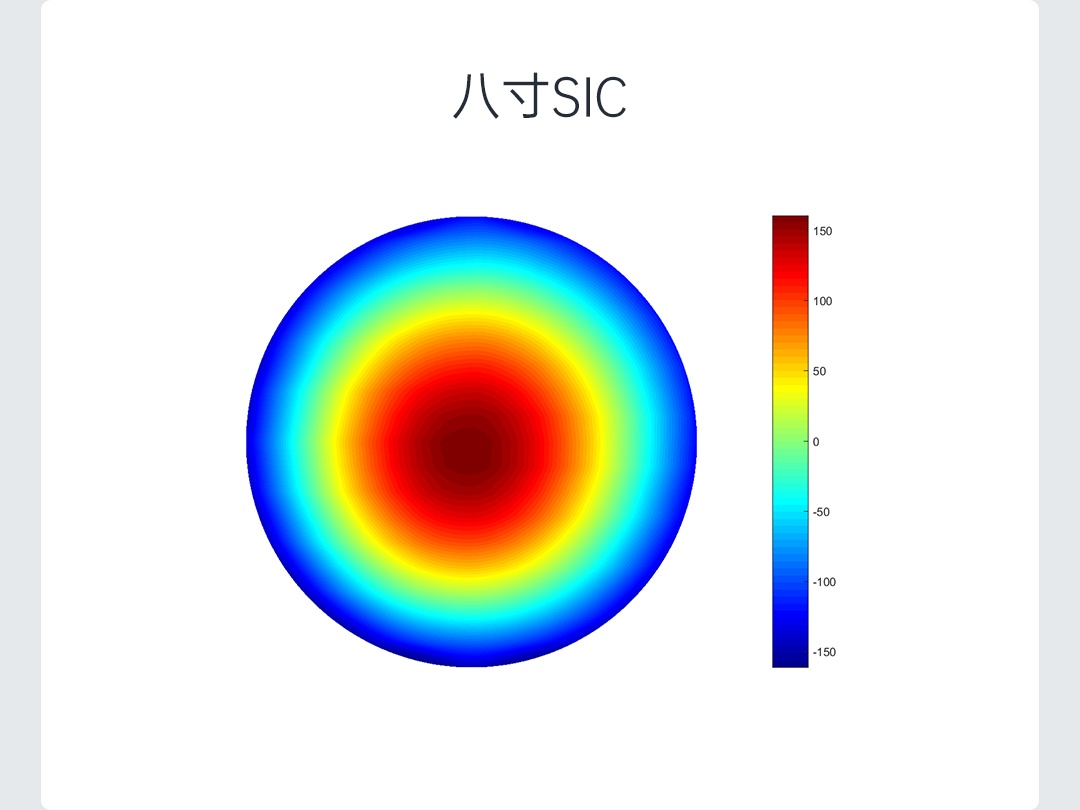
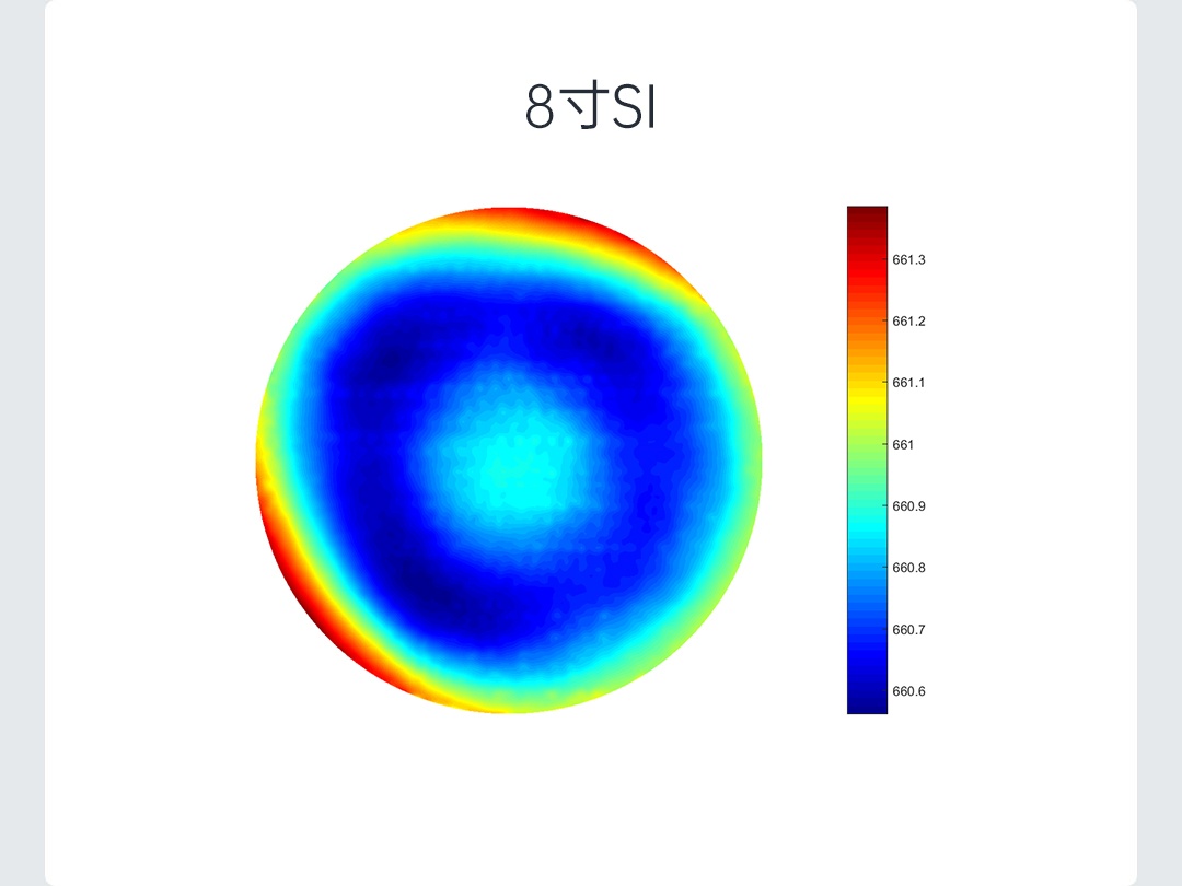
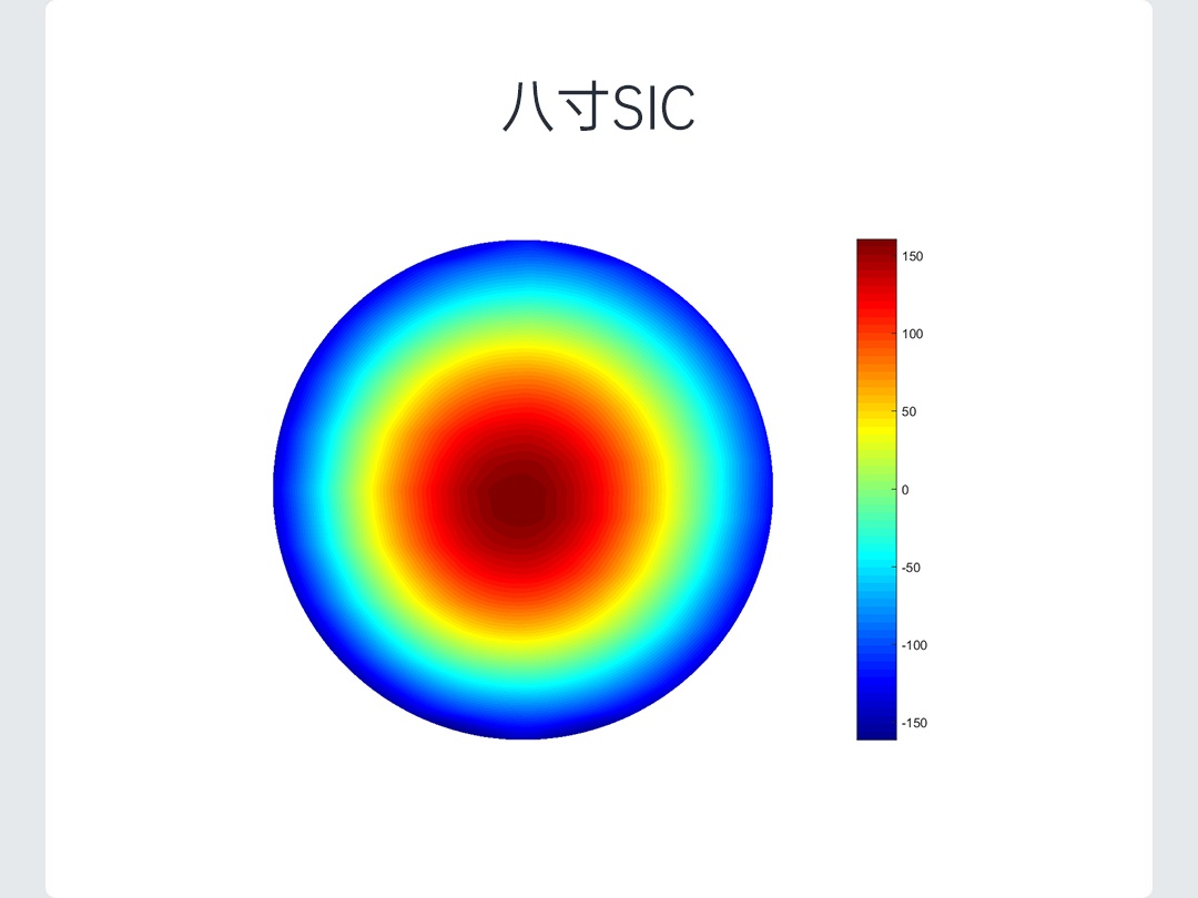
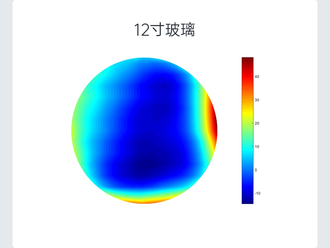
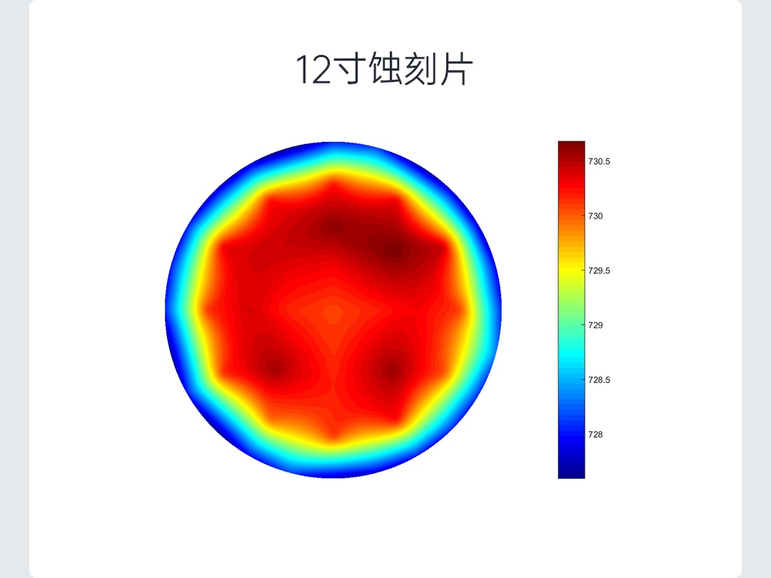
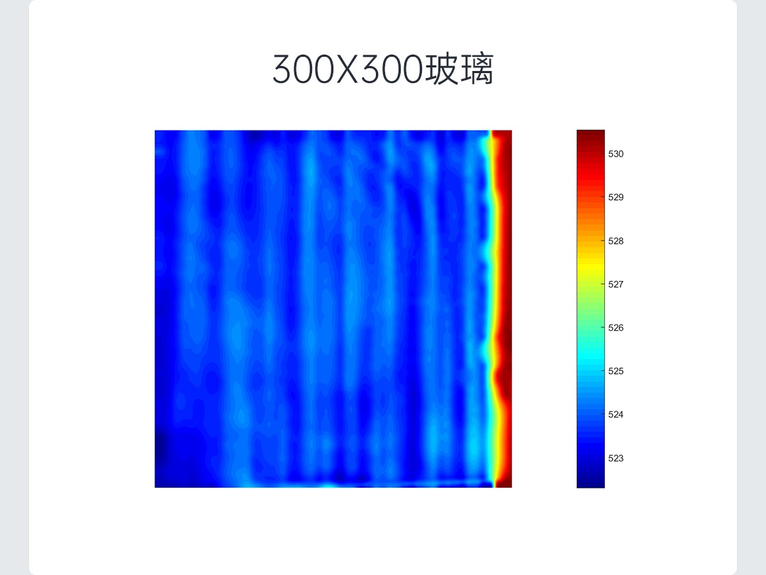
A single scan simultaneously captures all parameters—including thickness, TTV, Warp, and Bow—while generating a full-surface heat map of thickness and topography. This allows clients to intuitively assess the uniformity of the entire wafer. The complete inspection process takes less than two minutes, delivering improvements of over 60% in both inspection efficiency and data completeness compared to traditional contact-based measurement methods.
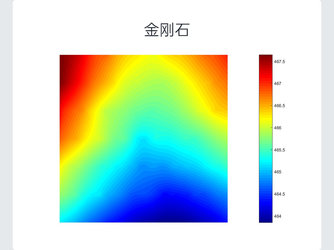
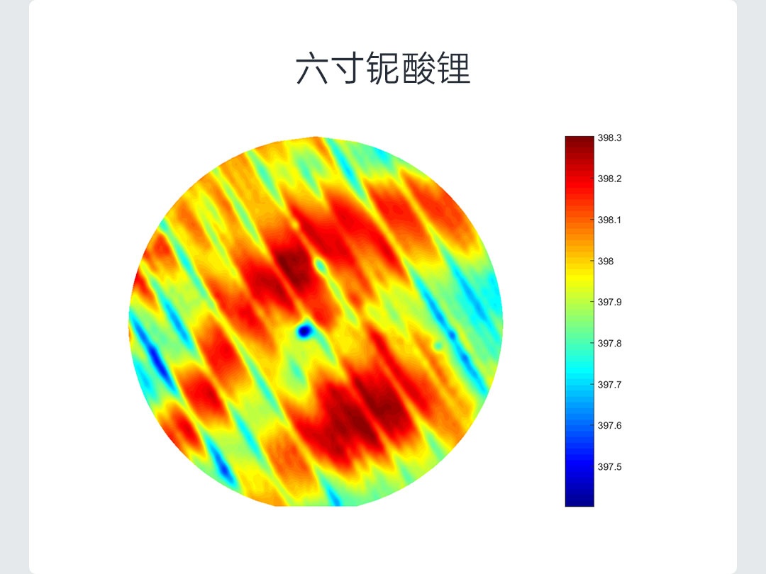
Beyond diamond wafers, the fully automated, non-contact thickness measurement system (APS) handles measurements for mainstream wafer specifications in a single unit:

Boardstone lntelligent(Shenzhen)Co.,Ltd.
6F Building C Kaifa Plaza,7006 Caitian Rd.,Futian Dist,Shenzhen
Hotline:400 080 3885
Sales@atometrics.com.cn
WhatsApp: +86 13316897904