Precision Inspection of Glass Substrates: Atometrics Solution Improves Yield to 90%
Atometrics' white light interferometer (0.03nm accuracy) & ultra-depth-of-field microscope – a high-precision inspection solution – helps improve the yield of glass substrates to 90%, accelerating the industry's high-end development.
The Rapidly Growing Glass Substrate Industry
In 2025, the Chinese glass substrate market size is expected to exceed RMB 37.1 billion, a year-on-year increase of 5.4%. This growth is mainly driven by demand from 3C consumer electronics such as smartphones and tablets. More importantly, the semiconductor packaging field is becoming a new growth engine – the global glass substrate packaging market is expected to reach USD 11.3 billion by 2031, with a compound annual growth rate of over 12%. This data reflects that glass substrates are extending from the traditional display field to high-value-added sectors, and their strategic value has gained industry consensus.
Technological Breakthrough – TGV Process
Among the core technological breakthroughs in glass substrates, TGV (Through Glass Via) technology is of milestone significance. This technology uses femtosecond laser-induced wet etching to create micron-sized vias, followed by copper/gold electroplating for vertical interconnects. Its key advantages include:
Ultra-low signal loss: The dielectric constant (Dk) of the glass substrate is below 4.0, more than 30% lower than traditional organic substrates, significantly improving the transmission efficiency of 5G/6G high-frequency signals;
Thermodynamic compatibility: The coefficient of thermal expansion (CTE) of the glass and silicon chip matches by 98%, eliminating packaging warpage caused by thermal stress in large-size AI chips (such as HBM memory);
3D integration potential: Supports micro-via fabrication below 50μm, providing a physical carrier for 2.5D/3D heterogeneous integration and meeting the transistor density breakthrough requirements of computing chips.
Currently, this technology has been applied to advanced packaging solutions for NVIDIA H100 GPUs and Apple M-series processors, increasing single-chip integration density by up to 40%.
Testing Needs
To support the industrialization of glass substrates, a precision testing system is crucial for technology implementation. Manufacturers need to measure surface morphology, internal roughness, line height and linewidth, and also observe defects and foreign matter within vias.
Atometrics testing solutions provide quantitative data for TGV process optimization, helping companies build a closed-loop quality control system and increasing product yield from the initial 60% to over 90%.
Atometrics Testing Solutions
I. The Atometrics AM series white light interferometer is used for internal roughness measurement, TGV sample morphology deformation analysis, line width and line height measurement, and substrate surface morphology measurement. It solves the problems of insufficient accuracy, low measurement efficiency, and inability to image highly transparent samples found in traditional equipment.
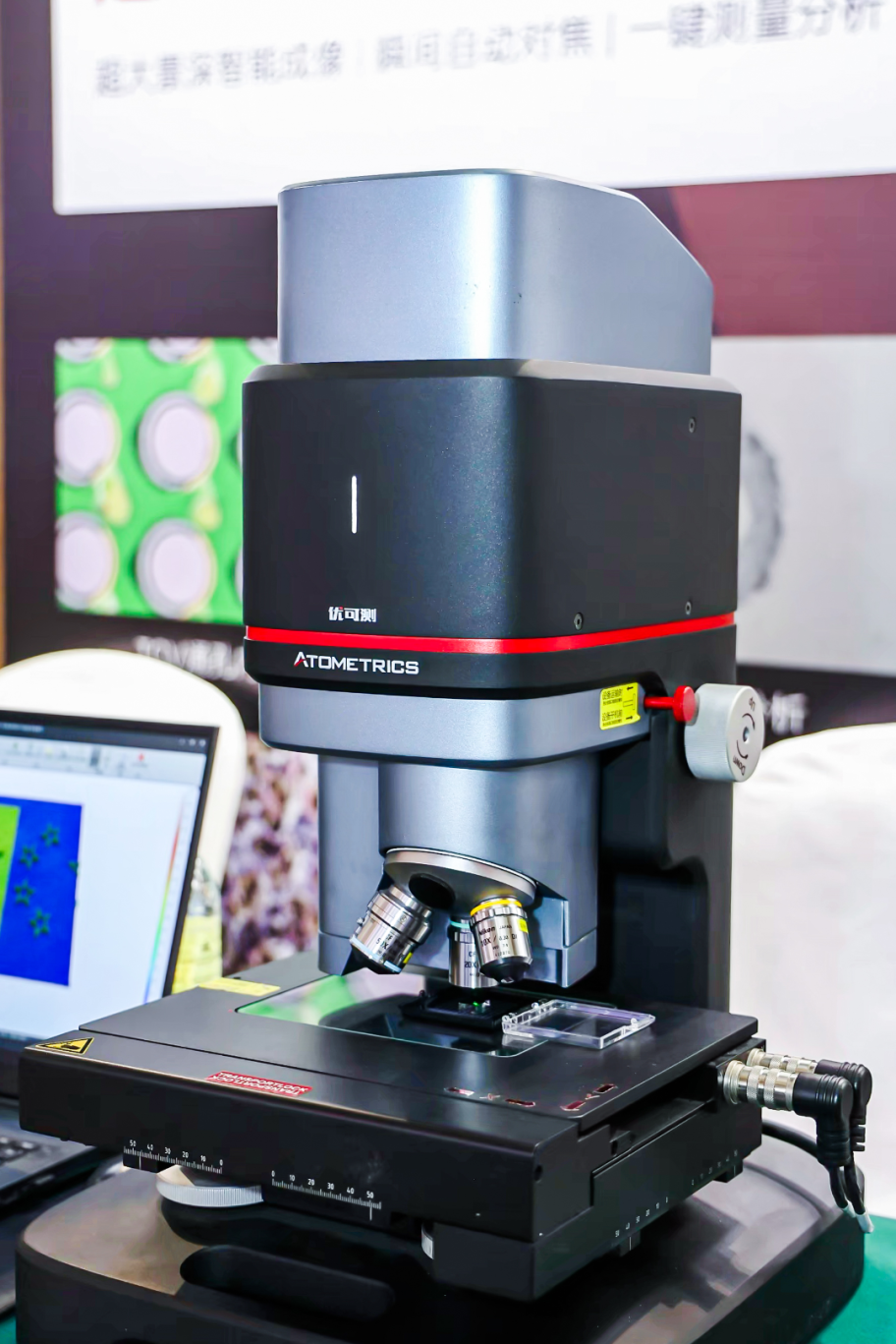
Atometrics AM Series White Light Interferometer
Key Advantages:
* **Ultra-High Precision:** Equipped with a closed-loop feedback piezoelectric ceramic material scanner (PZT), achieving Z-axis resolution with a precision up to 0.03nm;
* **Ultra-High Fidelity:** Equipped with a 2.3MP/5MP research-grade camera, enabling extremely accurate reproduction of sub-nanometer surface morphology;
* **Ultra-High Speed:** The proprietary SST/GAT algorithm allows for scanning speeds up to 400um/s;
* **Core R&D Strength in Software and Hardware:** Standard and non-standard solutions are available for large-format boards.
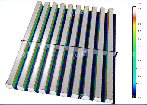
* **RDL Sample Surface Morphology Measurement**
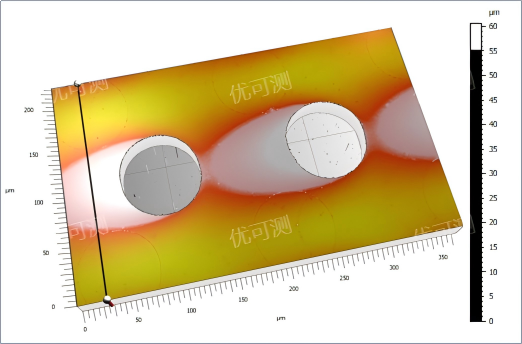
* **TGV Sample Surface Morphology Measurement**
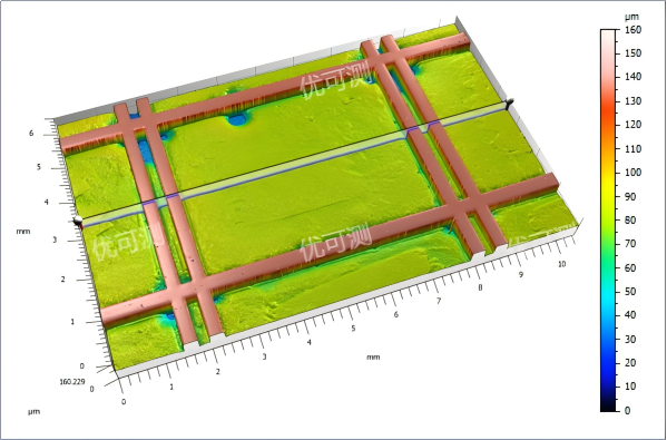
* **Substrate Sample Surface Morphology Measurement**
II. Atometrics AH Series Ultra-Depth-of-Field Microscope:** Used for laser drilling analysis, electroplating observation, circuit observation and measurement, solving problems associated with traditional metallographic and stereomicroscope observations such as small working distance, cumbersome focusing, inability to achieve side observation, and unclear images at high magnification.
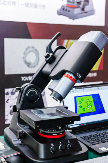
Atometrics AH Series Ultra-Depth-of-Field Microscope
Key Advantages:
High Resolution: 12 million effective pixels for ultra-high-definition observation;
Multi-Angle Observation: 90° left and right angles combined with a 270° platform rotation for omnidirectional multi-angle observation;
Telecentric Lens: Ensures measurement consistency across all magnifications;
Depth synthesis is possible at each magnification level with 12 million pixels, achieving high-definition observation at every magnification;
Split-Screen Observation: Real-time comparative analysis and automatic report output;
Ultra-High Working Distance: Prevents sample collision during tilted observation.
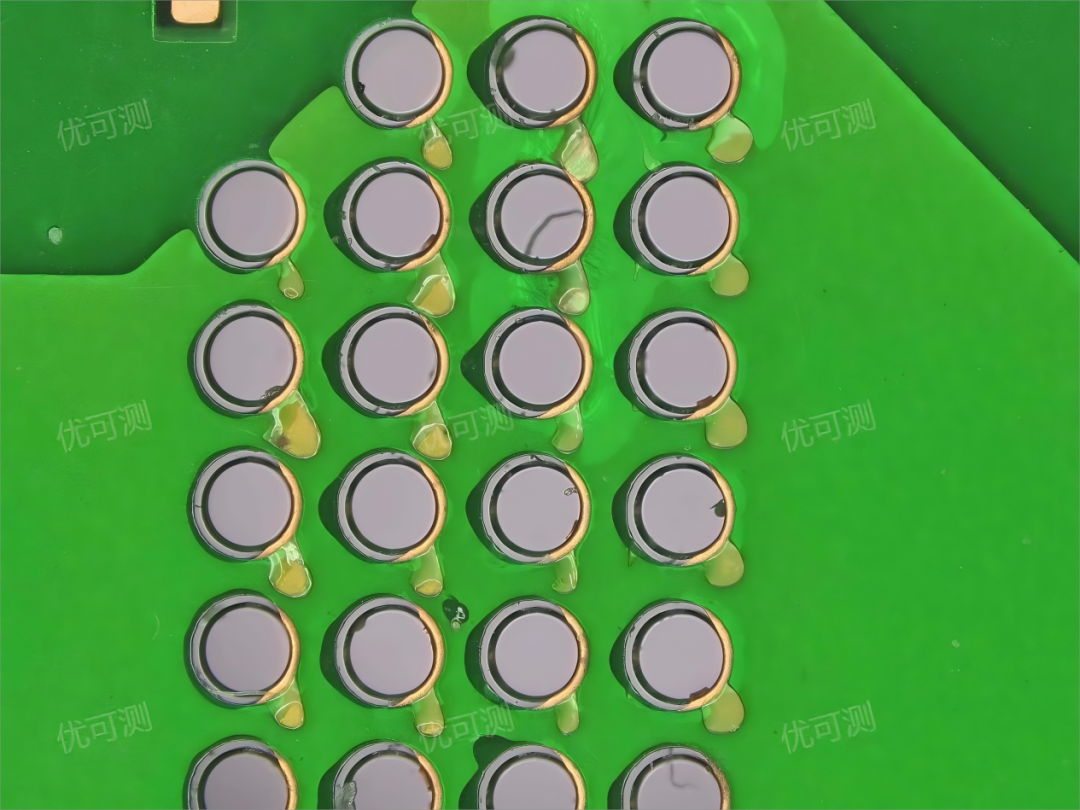
TGV Through-Hole Inner Wall Observation
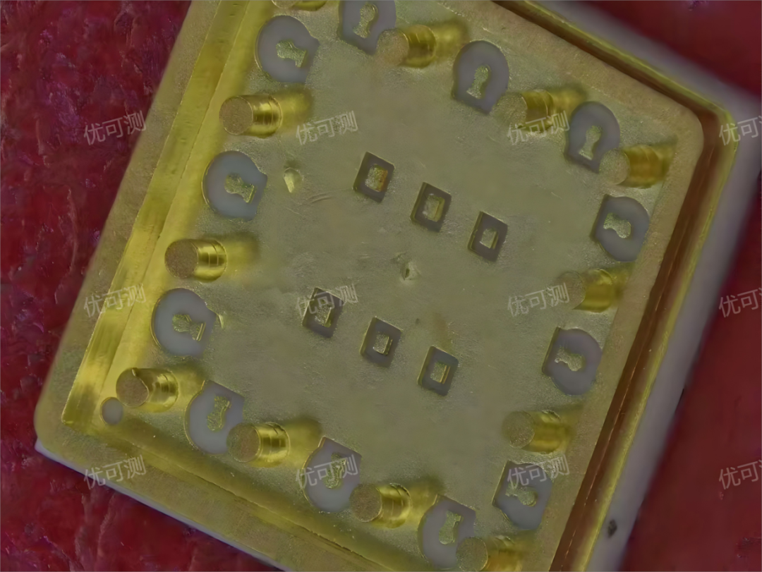
Substrate Surface Morphology Analysis
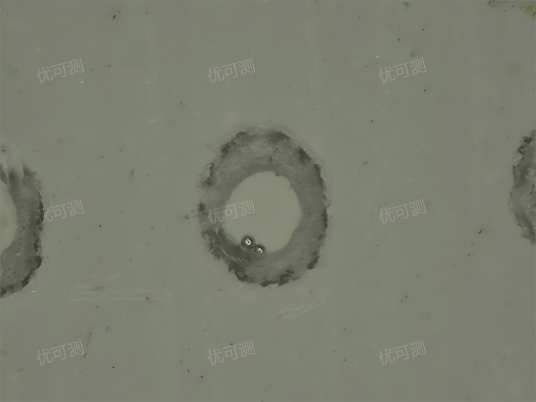
TGV Foreign Object Analysis
For any precision testing needs,
please call the Atometrics official technical hotline 400-0803885 or visit Atometrics official website.
Atometrics engineers will prioritize providing you with the best testing solution!

Boardstone lntelligent(Shenzhen)Co.,Ltd.
6F Building C Kaifa Plaza,7006 Caitian Rd.,Futian Dist,Shenzhen
Hotline:400 080 3885
Sales@atometrics.com.cn
WhatsApp: +86 13316897904