With the continuous advancement of technology, the field of chip manufacturing is gradually transitioning from the micrometer era to the nanometer era. Many high-tech enterprises are relentlessly pursuing excellence in technological innovation within these microscopic dimensions. In current mainstream chip manufacturing, photolithography is one of the core technologies for creating intricate circuit patterns.
The formation of photolithographic patterns is inseparable from the application of photoresist. There are three primary methods for coating photoresist onto wafers: Spin Coating, Film Lamination, and Spray Coating. Among these, spin coating technology is the most widely applied. Today, Atometrics explores the intricacies behind photoresist spin coating with you!
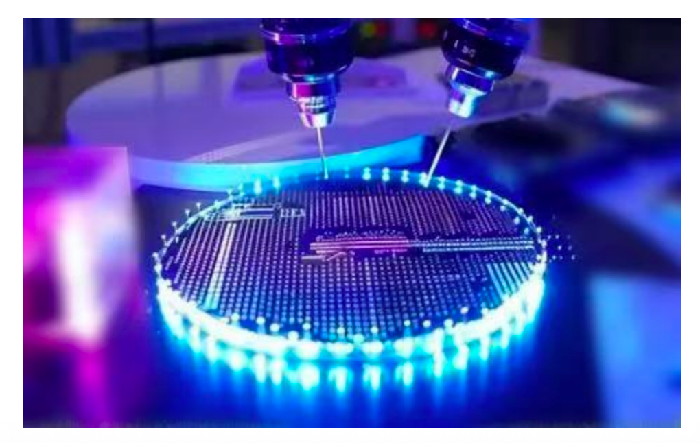
Photoresist Spin Coating
The Cornerstone of the Photolithography Process
Photoresist spin coating primarily involves applying photoresist by rotating the substrate. Different photoresists have specific requirements for process parameters such as temperature, photoresist thickness, and rotational speed.
The photolithography process flow mainly includes: Substrate Preparation → Photoresist Spin Coating → Soft Bake → Alignment and Exposure → Post-Exposure Bake → Development → Hard Bake → Inspection.
Photoresist spin coating occurs at the initial stage of the process. It provides a uniform photosensitive medium for subsequent steps like exposure, ensuring consistent photosensitivity effects across the exposed areas.
Monitoring Spin Coating Thickness
Ensuring Photolithography Pattern Accuracy
Statistical data shows that for every 1% reduction in chip scrap rate caused by poor photoresist spin coating, chip manufacturing companies can save millions of dollars annually. A minute error can lead to a massive discrepancy. Monitoring photoresist spin coating thickness plays a crucial role in the quality and efficiency of the entire chip manufacturing process.
During the exposure step, photoresist thickness is directly related to the amount of light absorbed during the process. According to the optical absorption law, variations in photoresist thickness lead to non-uniform light absorption, subsequently causing issues such as widening or deformation of the exposed lines.
During the etching step, the photoresist must protect areas that should not be etched. If the thickness is insufficient, the photoresist may fail to withstand the etchant's erosion, leading to damage in areas that should remain intact. If the thickness is excessive, it can easily trap residues, which similarly adversely affects the circuit structure. A 2020 study published in the Semiconductor Technology journal pointed out that during the etching process, for every 1% increase in the uniformity deviation of photoresist thickness, the line width deviation of the circuit pattern after etching increases by 3%-5%. This demonstrates the significant impact of photoresist thickness on etching precision.
Thickness Monitoring for Photoresist Spin Coating
Single-Point Measurement Time < 0.5s
To ensure the accuracy of photolithographic circuit patterns, a semiconductor client needed to monitor photoresist thickness on the production line with nanometer-level precision requirements, while also maintaining measurement efficiency.
Addressing the client's needs, we employed the Atometrics Film Thickness Measurement Instrument AF-3000 Series to build a Mapping solution for them: rapidly analyzing the uniformity of photoresist and etch thickness, and providing direction for process adjustments.
The AF Series Film Thickness Measurement Instrument abandons traditional LED light sources in favor of "Deuterium" and "Tungsten Halogen" lamps, which offer uniform light intensity and a stable spectrum. It supports measuring single-layer films, multi-layer films (up to 10 layers), liquid films, air-gap layers, and rough/smooth layers. One instrument covers the measurement range of multiple machines, delivering more precise results.
Actual testing has shown that the AF Series achieves a measurement accuracy of 0.1nm, a goodness-of-fit (Matching Degree) of 0.308420, and a single-point measurement time of < 0.5s. This fully meets the client's requirements for both measurement precision and efficiency, successfully helping the client save on photoresist costs, improve inspection efficiency, and enhance product yield during the photoresist coating stage!
The advanced film thickness metrology system offers you a brand-new experience.

Boardstone lntelligent(Shenzhen)Co.,Ltd.
6F Building C Kaifa Plaza,7006 Caitian Rd.,Futian Dist,Shenzhen
Hotline:400 080 3885
Sales@atometrics.com.cn
WhatsApp: +86 13316897904


